 main menu
| module menu
| << previous section
| next section >>
main menu
| module menu
| << previous section
| next section >>
Sentaurus Process
16. Special Focus: AlGaN Process Simulation
16.1 Overview
16.2 Substrate Definition
16.3 Deposition
16.4 Ion Implantation
16.5 Epitaxy, and Dopant Diffusion and Activation
16.6 Application Example: AlGaN p-Gate HFET
Objectives
- To demonstrate how to perform process simulations for AlGaN on SiC substrates.
16.1 Overview
Sentaurus Process can simulate most steps in the processing of AlGaN HFETs. Its capabilities include:
- Definition of growth orientation
- Deposition of layers
- Ion implantation
- Epitaxy of layers
This section discusses special settings required to perform AlGaN process simulations.
16.2 Substrate Definition
This section describes how to define the substrate.
16.2.1 Substrate Specification
AlGaN HFETs are grown on various substrates. Typical wafers are sapphire, silicon, SiC, and AlGaN. The first few layers of deposited materials are usually full of dislocations and other imperfections. These layers cannot be simulated in physical detail. Therefore, such layers are deposited simply as relaxed materials. The crystal directions of the deposited layers are assumed to follow the orientation set by the wafer and flat orientations in the init command.
16.2.2 Wafer and Flat Orientations
The wafer orientation and the flat orientation settings are similar to those for silicon. However, the hexagonal crystal system must be taken into account. In such crystals, four Miller indices are used to define a direction: a1, a2, a3, and c. However, a1, a2, and a3 depend on each other with the relationship: a1 + a2 + a3 = 0. Therefore, it is sufficient to use only three of the four Miller indices to determine any direction.
Sentaurus Process uses a1, a2, and c to define a direction, omitting the third Miller index. To specify the wafer and flat orientations, use the init command:
init wafer.orient= {a1 a2 c} notch.direction= {a1 a2 c}
The default wafer orientation is [0001], which is specified as wafer.orient= {0 0 1}. Almost all III–nitride HFETs are grown in this so-called Ga-face orientation, where the topmost layer is a Ga layer. Due to the polarization effect in such materials, it is important to specify the correct orientation, especially for device simulations.
In Sentaurus Process, possible flat orientations for such wafers are [1100] specified as notch.direction= {1 -1 0} and [1120] specified as notch.direction= {1 1 0}. The various directions in the hexagonal GaN lattice are shown in Figure 1.
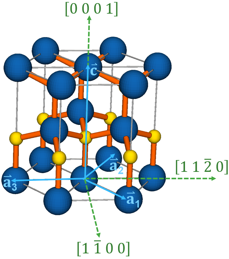
Figure 1. Important directions in the hexagonal GaN lattice. (Click image for full-size view.)
For further details about the hexagonal crystal system, see Section 15.2 Substrate Definition.
16.3 Deposition
Deposition of AlxGa1–-xN is performed similarly to the deposition of SiGe. Therefore, the mole fraction is set by the xMoleFraction field. In analogy to doping profiles, linearly graded mole-fraction profiles can be defined by their initial and final values:
doping  name= xMole field="xMoleFraction" depths= {0 $h_rel1} \
  values= "$xMoleRelax1 $xMoleRelax1"
deposit material= AlGaN region.name= relax1 thickness=$h_rel1 doping= {xMole}
In one dimension and two dimensions, Sentaurus Process automatically merges neighboring layers of the same material. To avoid such region-merging, you can set like materials, which are derived from a known material type. With the additional alt.matername argument, the new material is converted back to that material when saved for later device simulation. An example of such a new derived material is given here (not all information can be inherited for like materials):
mater add name= AlGaNbarrier new.like= AlGaN alt.matername= AlGaN
16.4 Ion Implantation
Sentaurus Process supports only Monte Carlo (MC) implantation into III–nitrides. There are no analytic tables. No extensive calibration of MC implantation parameters has been performed so far. Implanted dopants such as Si and Mg are rarely used for AlGaN HFETs.
MC implantation can be performed with:
implant <species> dose=<n> energy=<n> tilt=<n> particles=<n> sentaurus.mc
The number of particles specified is per 50 nm of the wafer width, not the total number of particles. In general, at least 2000 particles must be implanted to obtain reasonable statistics. For complicated geometries, as many as 10 000 particles might be needed.
Sentaurus MC implantation can be slow, so it is advisable to run it using parallel processing with:
math numThreadsMC=<i>
16.5 Epitaxy, and Dopant Diffusion and Activation
Dopants diffuse in AlGaN by interstitial and vacancy mechanisms as in silicon. However, little data exists for interstitial and vacancy components of dopant diffusivities in AlGaN, which complicates the calibration of such models. As an alternative phenomenological approach, you can use macroscopic diffusivity values to utilize a diffusion model with constant diffusivities. Such a constant diffusion model can be set for a certain dopant in a given material as:
pdbSet $material $Dopant DiffModel Constant
Sentaurus Process uses the Constant diffusion model for dopants (for example, Si and Mg) in the AlGaN material system by default.
All of the necessary model parameters for the diffusion models (for example, for silicon in AlGaN) can be initialized by single commands such as:
SetIIIVDiffParams AlGaN Silicon
The provided model parameters act only as a template. They are not calibrated. The diffusivities for the Constant diffusion model can be set explicitly with pdbSet commands, for example:
pdbSet GaN Silicon   Dstar {[ Arrhenius 6.66e-2 3.44]}
pdbSet GaN Magnesium Dstar {[ Arrhenius 5.00e-7 2.13]}
By default, Sentaurus Process uses the Solid model for dopant activation in GaN, AlN, and AlGaN, which assumes that dopants activate and deactivate to solid solubility values instantly. The model can be set explicitly together with the solubility for a given material dopant pair by:
pdbSet $material $Dopant ActiveModel Solid
pdbSet $material $Dopant Solubility 1e30
For mechanical stress calculation, you can use the lattice mismatch model. This model requires a reference position for the calculation of strain and stress, named TopRelaxedNodeCoord. At that reference position, the strain and stress are relaxed. The strain and stress at other positions are computed according to the difference in the lattice constant between the reference and that position. The TopRelaxedNodeCoord is set inside the relaxed layer material by:
pdbSetDouble <material> Mechanics TopRelaxedNodeCoord <position>
Relaxed layers towards the substrate are usually simulated with the deposit command. No dopant diffusion will occur during the deposition.
Strained layers or layers for which dopant out-diffusion might be important are grown epitaxially using the diffuse command, for example:
diffuse iiiv.epi= GaN time= 1.0 temp= $DiffTemp epi.thick= $h_barr \
  epi.doping= "[MoleFractionFields AlGaN $xMoleBarr] Magnesium= $pDensBarr \
                Silicon= $nDensBarr" \
  epi.doping.final= "[MoleFractionFields AlGaN $xMoleBarr]  \
                      Magnesium= $pDensBarr Silicon= $nDensBarr" \
  epi.model= 0 epi.layers= 10 info= 0
For the given project, these are the strained barrier layer and the highly doped p-type GaN gate material.
16.6 Application Example: AlGaN p-Gate HFET
This section presents a process simulation of a p-gate HFET device as part of the project Applications_Library/GettingStarted/sdevice/pGate_HFET.
See Section 16. Special Focus: Simulating AlGaN Devices With Sentaurus Device for a description of the device simulation part of this example.
Click to view the process command file sprocess_fps.cmd.
In the first part of the process flow, the diffusion and activation model settings as well as the parameter settings are specified for the III–nitride materials and dopants used:
foreach Dopant "Silicon Magnesium" {
  foreach material "GaN AlN AlGaN" {
      SetIIIVDiffParams $material $Dopant
      pdbSet $material $Dopant DiffModel Constant
      pdbSet $material $Dopant ActiveModel Solid
      pdbSet $material $Dopant Solubility 1e30
  }
}

pdbSetBoolean AlGaN_GaN Silicon   Continuous 1
pdbSetBoolean AlGaN_GaN Magnesium Continuous 1


pdbSet GaN Magnesium Dstar {[ Arrhenius 5.00e-7 2.13]}
pdbSet AlN Magnesium Dstar {[ Arrhenius 5.00e-7 2.13]}
pdbSet GaN Silicon   Dstar {[ Arrhenius 6.66e-2 3.44]}
pdbSet AlN Silicon   Dstar {[ Arrhenius 6.66e-2 3.44]}
The remaining model settings are for the mechanical simulation. The model for materials with anisotropic elastic properties are activated by:
foreach material "GaN AlGaN AlN" {
    pdbSetBoolean $material Mechanics Anisotropic 1
}
Mole fraction dependency for mechanical constants is switched on by:
pdbSet Mechanics Compound.Interpolation 1
After defining the settings for the base materials, like materials are defined. As previously mentioned, this helps to prevent automatic merging of adjacent layers of the same material:
mater add name= AlGaNbarrier     new.like= AlGaN  alt.matername= AlGaN
mater add name= GaNchannel       new.like= GaN    alt.matername= GaN
mater add name= AlGaNbuffer      new.like= AlGaN  alt.matername= AlGaN
mater add name= AlGaNrelax2      new.like= AlGaN  alt.matername= AlGaN
mater add name= AlGaNrelax1      new.like= AlGaN  alt.matername= AlGaN
mater add name= AlNnucleation    new.like= AlN    alt.matername= AlN
Then, the substrate definition is performed. The wafer is 4H-SiC, with a wafer orientation of [0001], a flat orientation of [1120], and a 4° miscut towards the wafer flat:
line x loc = $x0         tag= rTop    spacing= 0.3
line x loc = $h_SiC+$x0  tag= rBottom spacing= 0.3

line y loc = $ys  tag= rLeft  spacing= 0.05
line y loc = $Yd  tag= rRight spacing= 0.05

region SiliconCarbide xlo= rTop xhi= rBottom ylo= rLeft yhi= rRight name= wafer

init field= Nitrogen concentration=$ndopSiC  \
     wafer.orient= {@[split @WaferDirection@ ":"]@} \
     notch.direction=  {@[split @SliceDirection@ ":"]@} slice.angle= 0.0
On the SiC wafer, a 5 nm thick AlN nucleation layer is deposited, followed by a 250 nm Al0.5Ga0.5N layer and an Al0.25Ga0.75N layer of the same thickness. On top of that layer sequence, an Al0.05Ga0.95N buffer layer is deposited. The interface queries are performed to determine the top coordinates of the various layers:
deposit material= AlNnucleation region.name= nucleation thickness=$h_nuc
fset xnuc  [lindex [interface y= 0 AlN /Gas] 0]

doping  name= xMole   field="xMoleFraction" depths= {0 $h_rel1} \
  values= "$xMoleRelax1 $xMoleRelax1"
deposit material= AlGaNrelax1 region.name= relax1 thickness=$h_rel1 \
  doping= { xMole }
fset xrel1  [lindex [interface y= 0 AlGaNrelax1 /Gas] 0]

doping  name= xMole   field="xMoleFraction" depths= {0 $h_rel2} \
  values= "$xMoleRelax2 $xMoleRelax2"
deposit material= AlGaNrelax2 region.name= relax2 thickness=$h_rel2 \
  doping= { xMole }
fset xrel2  [lindex [interface y= 0 AlGaNrelax2 /Gas] 0]

doping  name= xMole   field="xMoleFraction" depths= {0 $h_buf} \
  values= "0.05 0.05"
deposit material= AlGaNbuffer region.name= buffer thickness=$h_buf \
  doping= { xMole }
fset xbuf  [lindex [interface y= 0 AlGaNbuffer /Gas] 0]
After the deposition of these layers, the TopRelaxedNodeCoord for the lattice mismatch model is specified to point into the relaxed channel layer to be deposited next:
fset topcoord [expr 1e-4*($xbuf-$h_cha/2.)]
pdbSetDouble GaNchannel Mechanics TopRelaxedNodeCoord $topcoord

doping  name= dopcha field= "Magnesium" depths= {0 $h_cha} \
  values= "$DensCha $DensCha"
deposit material= GaNchannel region.name= channel thickness=$h_cha \
  doping= { dopcha }
fset xcha  [lindex [interface y= 0 GaNchannel /Gas] 0]
region name= channel substrate
The channel layer will act as the substrate for the subsequent epitaxial steps. As such, this region must be marked with the substrate flag.
The strained barrier layer is now grown pseudomorphically on to the GaN channel with a corresponding diffuse command:
fset DiffTemp 600
diffuse iiiv.epi= GaN time= 1.0 temp= $DiffTemp epi.thick= $h_barr \
  epi.doping= "[MoleFractionFields AlGaN $xMoleBarr] \
    Magnesium= $pDensBarr Silicon= $nDensBarr" \
  epi.doping.final= "[MoleFractionFields AlGaN $xMoleBarr] \
    Magnesium= $pDensBarr Silicon= $nDensBarr" \
  epi.model= 0 epi.layers= 10 info= 0
fset xbarr  [lindex [interface y= 0 AlGaN /Gas] 0]
region new.name=alganbarrier point= "[expr ($xcha+$xbarr)/2] 0"
region name= alganbarrier change.material  AlGaNbarrier !zero.data
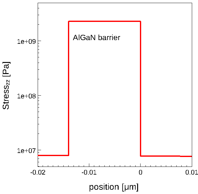
Figure 2. In-plane stress zz component after pseudomorphic growth of Al0.25Ga0.75N barrier layer onto relaxed GaN. (Click image for full-size view.)
After deposition of the AlGaN barrier layer, its material is changed to the like material alganbarrier. The option !zero.data instructs Sentaurus Process to keep the solution variables in that region. Otherwise, they would be set to zero.
Next, a highly magnesium-doped p-gate GaN layer is grown, which will form the p-gate of the device:
diffuse iiiv.epi= GaN time= 1.0 temp= $DiffTemp epi.thick= $h_barr \
  epi.doping= "[MoleFractionFields AlGaN $xMoleBarr] \
    Magnesium= $pDensBarr Silicon= $nDensBarr" \
  epi.doping.final= "[MoleFractionFields AlGaN $xMoleBarr] \
    Magnesium= $pDensBarr Silicon= $nDensBarr" \
  epi.model= 0 epi.layers= 10 info= 0
fset xbarr  [lindex [interface y= 0 AlGaN /Gas] 0]
region new.name=alganbarrier point= "[expr ($xcha+$xbarr)/2] 0"
region name= alganbarrier change.material  AlGaNbarrier !zero.data


# epi growth of p-gate layer
diffuse iiiv.epi= GaN time= 1.0 temp= $DiffTemp epi.thick= $h_ggan \
        epi.doping= "Magnesium= $pgateMg" \
        epi.model= 0 epi.layers= 30 info= 0
fset xgate  [lindex [interface y= 0 GaN /Gas] 0]
region new.name= pgate point= "$xgate+0.001"
Some of the magnesium will out-diffuse from that layer into the barrier layer during its epitaxial growth, as shown in Figure 3.
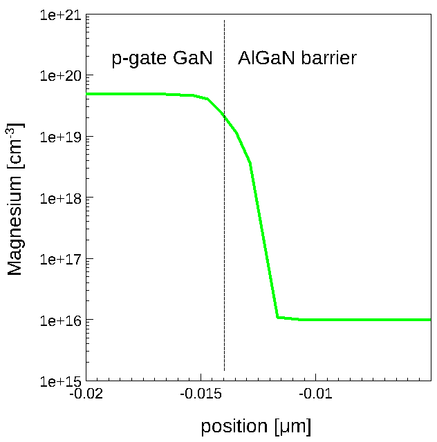
Figure 3. Magnesium profile after p-gate GaN epitaxy. (Click image for full-size view.)
The remaining process steps are standard mask, etching, and deposition steps to adjust the p-gate length and to form the metallic regions of the contacts, described in Section 3.5 Defining Polysilicon Gate and Section 3.13 Contact Pads.
The trap profiles present in such structures are not the result of the simulation. If such profiles should be included in the device simulation, user-defined PMIUserField0, PMIUserField1, ... profiles can be added with select commands, for example:
select AlNnucleation name= "PMIUserField0" z="1e19" store
select AlGaNrelax1   name= "PMIUserField0" z="2e18" store
select AlGaNrelax2   name= "PMIUserField0" z="1e18" store
select AlGaNbuffer   name= "PMIUserField0" z="(x>$xbuf+0.5) ? (1e18) : \
  (1e15+(1e18-1e15)*exp(-($xbuf+0.5-x)/0.1))" store
select GaNchannel    name= "PMIUserField0" z="(x>$xbuf+0.5) ? (1e18) : \
  (1e15+(1e18-1e15)*exp(-($xbuf+0.5-x)/0.1))" store
Figure 4 shows the resulting profile of this example. The PMIUserFields can be used in Sentaurus Device together with SFactor=PMIUserField0, as discussed in Section 13.4 Trap Spatial Distribution.
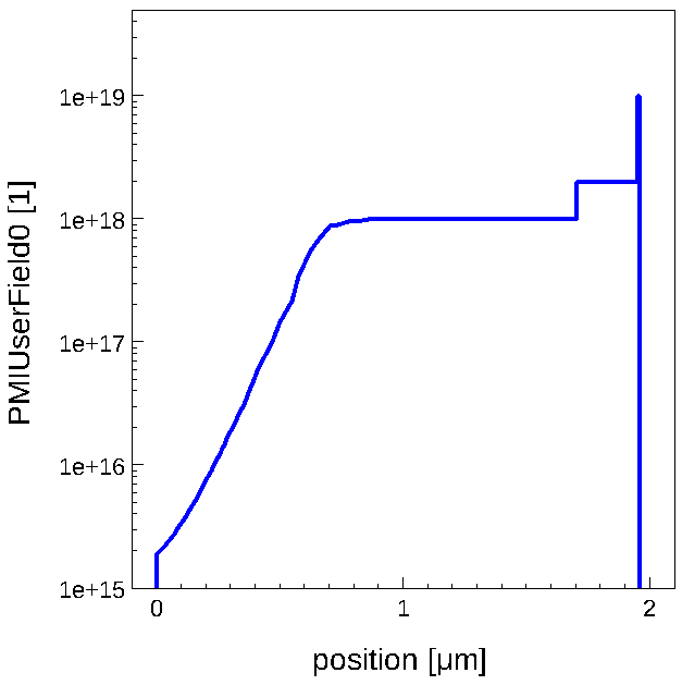
Figure 4. User-defined PMIUserField0 profile. (Click image for full-size view.)
Finally, the device is meshed for device simulations and the contacts are defined. Refer to the Sentaurus Process module, Section 10. Special Focus: Remeshing for Device Simulation for details about this step.
Figure 5 shows the final device structure.
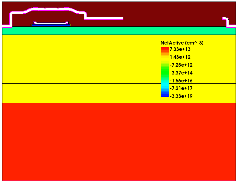
Figure 5. Final device structure to be simulated with Sentaurus Device. (Click image for full-size view.)
main menu | module menu | << previous section | next section >>
Copyright © 2022 Synopsys, Inc. All rights reserved.