
Sentaurus Device
16. Special Focus: Simulating AlGaN Devices With Sentaurus Device
16.1 Overview
16.2 AlGaN/GaN Parameter Files
16.3 Crystal and Device Orientation
16.4 III–Nitride-Specific Physical Models: Polarization Effects
16.5 Traps in III–Nitride Devices
16.6 AlGaN-Specific Numeric Parameters
16.7 Application Example: p-Gate AlGaN HFET
16.8 Application Example: GaN p-i-n Diode
16.9 Relevant Application Notes
Objectives
- To demonstrate the use of various polarization models implemented in Sentaurus Device.
- To demonstrate an Id–Vg simulation of a p-gate AlGaN HFET using Sentaurus Device.
16.1 Overview
This example follows the description of the project process part in Section 16. Special Focus: AlGaN Process Simulation and provides more insight into how to perform an AlGaN device simulation in conjunction with the AlGaN process simulation.
The complete project can be accessed from Sentaurus Workbench in the directory Applications_Library/GettingStarted/sdevice/pGate_HFET.
16.2 AlGaN/GaN Parameter Files
Dedicated parameter files for GaN, AlN, and AlGaN are provided in the $STROOT/tcad/$STRELEASE/lib/sdevice/MaterialDB/ directory. In addition, there are parameter files for the InGaN material family in the same location. Sentaurus Workbench provides an easy way to access these files. See Section 7.2 Customizing Tool Input File. For a general discussion on parameter specifications for ternary materials, see Section 4.2 Model Parameter Definitions for Nonsilicon Material.
In this example, the default GaN, AlN, and AlxGa1–xN files from the MaterialDB folder are used together with the SiC parameters discussed in Section 15.2 SiC Parameter Files. As an example, the band gap of AlxGa1–xN is shown in Figure 1.
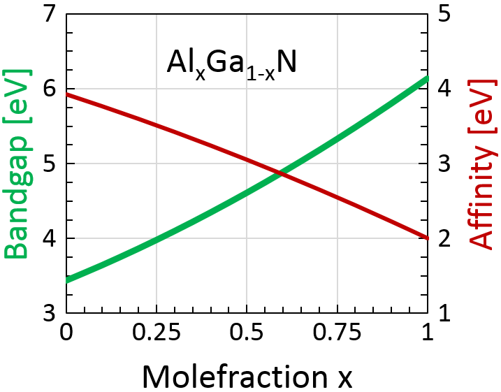
Figure 1. Band gap at 300 K (green line) and affinity (red line) of AlxGa1–xN as a function of mole fraction x. (Click image for full-size view.)
16.3 Crystal and Device Orientation
III–nitride materials in their wurtzite phase exhibit strong piezoelectric and spontaneous polarization effects. The spontaneous polarization is aligned parallel to the c-axis of the hexagonal crystal. Due to this intrinsic anisotropy, the orientation of the simulation coordinate system relative to the crystal is important.
This orientation is read from the TDR file and is used implicitly by Sentaurus Device if the device structure is computed by Sentaurus Process. Otherwise, the orientation of the simulation coordinate system with respect to the crystal must be specified in a LatticeParameters section in the parameter file of Sentaurus Device.
Any orientation read from a TDR file is overwritten by an explicit Sentaurus Device setting of the LatticeParameters section. It is recommended to use a single global LatticeParameters section for a given device simulation, if one is required.
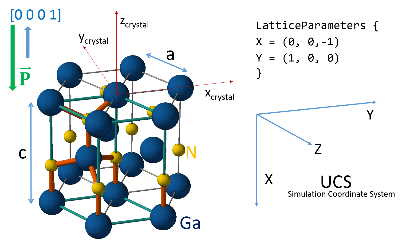
Figure 2. Hexagonal lattice of wurtzite GaN. Green connections indicate the primitive unit cell. The Ga–N bonds in the unit cell are orange. The crystal fixed Cartesian coordinate system is indicated in red. The given LatticeParameters setting orients the simulation x-axis of the UCS antiparallel to the c-axis of the crystal. (Click image for full-size view.)
The device coordinate system is oriented relative to the crystal coordinate system in the LatticeParameters section of the parameter file. Sentaurus Device assumes a Cartesian crystal coordinate system fixed to the semiconductor crystal. In wurtzite crystals, the orientation of this crystal coordinate system is such that the c-axis points along its z-axis. The x-axis and y-axis are oriented along <2110> and <0110>, respectively. Figure 2 shows the hexagonal GaN lattice together with such coordinate axes.
Typically, the c-axis of the crystal points vertically upwards in the simulation coordinate system. In the unified coordinate system (UCS), the x-axis always points downwards. The corresponding LatticeParameters section as shown in Figure 2 reads:
LatticeParameters {
  X = (0, 0,-1)
  Y = (1, 0, 0)
}
For the DF–ISE coordinate system in two dimensions, the y-axis points downwards. The corresponding LatticeParameters setting with the crystal c-axis pointing upwards reads:
LatticeParameters {
  X = (1, 0, 0)
  Y = (0, 0,-1)
}
For the DF–ISE coordinate system in three dimensions:
LatticeParameters {
  X = (0, -1, 0)
  Y = (1,  0, 0)
}
16.4 III–Nitride-Specific Physical Models: Polarization Effects
Sentaurus Device provides alternatives of different complexity to model polarization effects, ranging from the placement of explicit interface charges to full-volume polarization fields, computed from strain or stress distributions in the device.
16.4.1 Strain Model
The strain model is available in a general and a simplified version. Both versions are activated in the Physics section, for example:
Physics {
  Piezoelectric_Polarization (strain)
}
16.4.1.1 Full Strain Model
With the full strain model, the piezoelectric polarization vector is expressed as a function of the local strain tensor \(ε↖{-}\):
\[ [\table P_{x}; P_{y}; P_{z}] = [\table P_{x}^{\text"sp"}; P_{y}^{\text"sp"}; P_{z}^{\text"sp"}] + [\table e_{11}, e_{12}, e_{13}, e_{14}, e_{15}, e_{16}; e_{21}, e_{22}, e_{23}, e_{24}, e_{25}, e_{26}; e_{31}, e_{32}, e_{33}, e_{34}, e_{35}, e_{36} ] [\table ε_{xx}; ε_{yy}; ε_{zz}; ε_{yz}; ε_{xz}; ε_{xy} ] \]
Here, \(P^{\text"sp"}\) is the spontaneous polarization vector, and the quantities \(e_{ij}\) denote the strain-charge piezoelectric coefficients. The quantities \(P^{\text"sp"}\) and \(e_{ij}\) are defined in the crystal system. The polarization vector is first computed in crystal coordinates and is converted to simulation coordinates afterwards.
This general model is evaluated in either of the following circumstances:
- A constant strain tensor is specified in the Piezo section of the command file:
Physics { Piezo( Strain= (xx yy zz yz xz xy) ) } - The strain tensor is read from a TDR file. This requires the specification of:
Physics {
  Piezo( Strain= LoadFromFile )
}
and the specification of the corresponding TDR file within the File section of the command file:
File { Piezo= <file> }
16.4.1.2 Simplified Strain Model
The most popular III–nitride-based devices such as HFETs for RF and power-switching applications are built from epitaxial structures formed by multiple layers with the growth direction [0001] and constant mole fractions within each layer. In such structures, the primary effect of polarization is an interface charge (polarization charge) due to the abrupt divergence in the polarization at such III–nitride heterointerfaces.
The easiest way to model polarization in such epitaxial devices is to use the simplified strain model that computes spontaneous and piezoelectric components based on the local mole fraction and the strain resulting from the assumption of pseudomorphic growth onto a reference layer with a certain lattice constant, a0. For these simplifying assumptions, the strain model reduces to the simplified strain model, in which the total polarization is given by:
\[ [\table P_{x}; P_{y}; P_{z}] = [\table P_{x}^{\text"sp"}; P_{y}^{\text"sp"}; P_{z}^{\text"sp"} + P_{\text"strain"}] \]
where:
\(P_{\text"strain"} = 2d_{31} · \text"strain" ·(c_{11} + c_{12} - {2c_{13}^{2}} / {c_{33}}) \) , for Formula=1
\(P_{\text"strain"} = 2 · \text"strain" ·(e_{31} - e_{33} {c_{13}}/{c_{33}} ) \) , for Formula=2
\(\text"strain" = (1 - \text"relax") · ({a_{0} - a} / {a}) \)
Two equivalent models can be selected for the simplified strain model by the Formula keyword:
- For Formula=1, stress-charge piezoelectric coefficients \(d_{31}\) are used.
- For Formula=2, strain-charge coefficients \(e_{31}\) are used.
The Formula keyword is set in the Piezoelectric_Polarization parameter section together with the strained and unstrained in-plane lattice constants \(a_{0}\) ( a0) and \(a\) (a).
The simplified strain model provides a strain relaxation parameter relax in the Piezoelectric_Polarization parameter set. It is used to scale the piezoelectric polarization component due to stress relaxation as indicated in the formula above.
Piezoelectric_Polarization {
  formula   = 1

  * strain parameters:
  * a0: strained lattice constant [Angstrom]
  * a: unstrained lattice constant [Angstrom]

  a0  = 3.189 # [Angstrom]
  a = 3.179 # [Angstrom]

  * relax: relaxation parameter [1]
  relax   =   0.0
...
}
The setting relax=1 corresponds to a fully relaxed material and relax=0 specifies no stress relaxation.
16.4.2 Stress Model
The stress model computes the full polarization vector in tensor form, the general stress tensor σ, and the piezoelectric stress-charge coefficients as:
\[ [\table P_{x}; P_{y}; P_{z}] = [\table P_{x}^{\text"sp"}; P_{y}^{\text"sp"}; P_{z}^{\text"sp"}] + [\table d_{11}, d_{12}, d_{13}, d_{14}, d_{15}, d_{16}; d_{21}, d_{22}, d_{23}, d_{24}, d_{25}, d_{26}; d_{31}, d_{32}, d_{33}, d_{34}, d_{35}, d_{36} ] [\table σ_{xx}; σ_{yy}; σ_{zz}; σ_{yz}; σ_{xz}; σ_{xy} ] \]
The stress model is activated in the Physics section, for example:
Physics {
  Piezoelectric_Polarization (stress)
}
The stress tensor is read from the Piezo file specified in the File section of the Sentaurus Device command file:
File { Piezo= <file> }
16.4.3 Polarization Charge Scaling
The scaling factor activation allows you to scale the polarization charge at interfaces resulting from an abrupt change of the polarization. For example, the following region interface–specific Physics section would effectively switch off any polarization effects at the interface between regions relax1 and nucleation:
Physics (RegionInterface="relax1/nucleation") {
  Piezoelectric_Polarization(activation=0)
}
16.4.4 Polarization Parameter Set
Parameters to calculate the polarization fields in the device are given in material-specific or region-specific Piezoelectric_Polarization sections. The material-specific parameters for the AlGaN material system are included in the material library of Sentaurus Device, located at $STROOT/tcad/$STRELEASE/lib/sdevice/MaterialDB/. They are used by setting the keyword DefaultParametersFromFile in the Physics section:
Physics { DefaultParametersFromFile ...}
For GaN, some of the settings are given here:
Piezoelectric_Polarization {
  formula   = 1

  * strain parameters:
  * a0: strained lattice constant [Angstrom]
  * a: unstrained lattice constant [Angstrom]

  a0  = 3.189 # [Angstrom]
  a = 3.189 # [Angstrom]

  * relax: relaxation parameter [1]
  relax   =   0.0

  * piezoelectric coefficients, defined in crystal system [cm/V]:
  d15 =  3.1000e-10   # [cm/V]
  d24 =  3.1000e-10   # [cm/V]
  d31 =  ...
    ...

  * spontaneous polarization:
  psp_x =  0.0000e+00 # [C/cm^2]
  psp_y =  0.0000e+00 # [C/cm^2]
  psp_z = -3.4000e-06 # [C/cm^2]


  * stiffness constants:
  c11 = 3.9000e+11    # [Pa]
  c12 = ...
  ...

  * piezoelectric coefficients
  e31 = -5.2964e-05   #[C/cm^2]
  e32 = ...
  ...
}
16.4.5 Anisotropy
In addition to the intrinsic polarization anisotropy due to spontaneous polarization, material properties such as impact ionization and dielectric properties are expected to show some anisotropy. However, mainly for the lack of reliable data, only the latter is included more often in simulations.
In this example, only isotropic transport parameters are used. However, electrostatic anisotropy due to anisotropic dielectric properties can be activated optionally. For a thorough discussion of anisotropic model settings, see Section 15.3.3 Material Parameter Anisotropy.
To switch on a specific anisotropic model, the corresponding keyword must be placed in the Aniso subsection of the global Physics section. For anisotropic dielectric material parameters, the corresponding command is given by:
Physics {...
  Aniso (
    Poisson
    direction(SimulationSystem)= xAxis
  )
}
This results in anisotropy of the dielectric properties entering the Poisson equation, with the anisotropic axis along the x-axis of the simulation coordinate system.
16.5 Traps in III–Nitride Devices
Traps are present almost throughout AlGaN/GaN HFETs. Partially, they are induced already during imperfect growth of nucleation and following relaxation layers. Others are formed at the interfaces between semiconductor layers, at the passivation interface, or at the channel interface of GaN MOS structures, where they can cause non-idealities in C-V characteristics. All of these traps can have a significant influence on device behavior. However, profiles, trap types, and characteristics strongly depend on the details of the technology used.
For a discussion of trap models in Sentaurus Device, see Section 13. Special Focus: Traps.
16.5.1 Interface Traps
Interface traps in III–N device technology usually act as passivation centers, which effectively compensate the interface charge induced by the polarization. For example, the polarization change at the interface from the top AlGaN barrier layer to the passivation layer induces a large negative interface charge. The inclusion of passivating donor trap levels at that interface results in the capture of holes, which compensates the negative interface charge.
For a similar effect, acceptor trap levels are introduced at the nucleation–wafer interface. Such trap levels compensate the polarization-induced positive charge by capturing electrons.
An example of donor passivation traps at the barrier–nitride interface is:
Physics (RegionInterface= "alganbarrier/passivation_left") {
 Traps (( Donor Level fromCondBand EnergyMid= 0.4 Conc= 3e13
          eXsection=1e-14  hXsection=1e-14 ))
}
Physics (RegionInterface= "alganbarrier/passivation_right") {
 Traps (( Donor Level fromCondBand EnergyMid= 0.4 Conc= 3e13
          eXsection=1e-14  hXsection=1e-14 ))
}
The values used here do not represent exactly the values observed in experiments and might need to be adjusted to technology-specific or user-specific settings.
16.5.2 Bulk Traps
Throughout the different device layers, various bulk traps are present. Typically, the material quality improves along the epitaxial growth direction. However, nucleation, relaxation, and buffer layers can be full of imperfections at different levels.
By default, Sentaurus Device assumes constant trap distributions over given regions or materials. As an alternative, spatial trap distributions can be specified in Sentaurus Device. To consider such distributions, user-defined PMIUserField profiles (PMIUserField0, PMIUserField1, PMIUserField2, ...) can be declared in either a process simulation (see Section 16.6 Application Example: AlGaN p-Gate HFET) or Sentaurus Structure Editor. These fields are then read as specified in the File section of Sentaurus Device and are used with the SFactor option in the trap specification.
For details about the SFactor option, see Section 13.4 Trap Spatial Distribution.
16.5.3 Example: GaN MOS C–V Characteristics With Interface Traps Effects
To build high-quality GaN MOSFETs, understanding the non-idealities in C–V characteristics of a GaN MOS structure is an important step. The high-frequency and low-frequency responses of gate capacitance with respect to gate voltage provide information about the deep-level traps present in GaN devices. In general, the minority carrier response is extremely slow in wide-bandgap materials, such as GaN and SiC. The device simulation results with the quasistationary approach do not consider the time taken by the minority carriers and might give incorrect results.
In this project, the C–V characteristics of an n-type GaN MOS device are simulated with transient and quasistationary methods for both high-frequency and low-frequency conditions.
The complete project can be investigated from within Sentaurus Workbench in the directory Applications_Library/GettingStarted/sdevice/GaN_MOSCAP_1D.
16.5.3.1 Project Organization
Figure 3 shows the organization of the project in Sentaurus Workbench. The n-type GaN MOS device structure is generated using Sentaurus Structure Editor. To generate the C–V characteristics of the device, Sentaurus Device is used. The Sentaurus Workbench parameter dt is used to vary the gate voltage ramp rate in the transient simulation mode. Finally, the C–V characteristics are plotted using Sentaurus Visual.
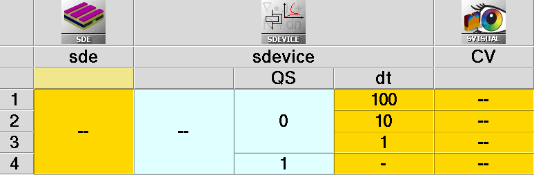
Figure 3. Project organization in Sentaurus Workbench, showing the flow from Sentaurus Structure Editor to Sentaurus Device to Sentaurus Visual. (Click image for full-size view.)
The following Sentaurus Workbench parameters are varied in the project:
- dt: Gate voltage ramp time from -5 V to +5 V, in transient method: 100, 10, and 1 [unit: s]
- QS: Flag to select transient or quasistationary simulation method: 0 = transient ; 1 = quasistationary
16.5.3.2 Device Structure Generation
To generate the 1D structure of the n-type GaN MOS device, Sentaurus Structure Editor is used. Two blocks of rectangles are defined: one for the Oxide region and one for the GaN region, doped at 2×2017 cm-3. The thickness of the Oxide region is defined as 10 nm. Contacts are placed at the top and bottom, and mesh refinements are specified.
Click to view the structure generation command file sde_dvs.cmd.
16.5.3.3 Device Simulation: C–V Characteristics
This section presents simulation details about the gate capacitance versus gate voltage characteristics of the device.
Electrical boundary conditions are defined in the Electrode section. Only the gate and source electrodes are present in the device. The gate metal contact with a workfunction value of 5.0 eV is defined. The Electrode section of the command file is:
  Electrode {
    { Name="gate"  Voltage= 0.0 Workfunction= 5.0}
    { Name="subs"  Voltage= 0.0 }
  }
In the File section, the input and output files required for the simulation process are defined:
  File {
    Grid= "@tdr@"
    Parameter= "@parameter@"

    Current= "@plot@"
    Plot= "@tdrdat@"
  }
To simulate the GaN MOS devices, the following models are used: Shockley–Read–Hall (SRH) recombination, Masetti mobility model to account for doping-dependent mobility degradation, Fermi–Dirac carrier statistics, and acceptor traps at the GaN–Oxide material interface.
A simplified strain-based piezoelectric polarization model is defined with an activation level of 5%, assuming that the majority of polarization charge is compensated by fixed charges at the GaN–Oxide interface.
The Physics section used in the command file is:
  Physics {
    AreaFactor= 5e8   * So capacitance given in F/cm^2
    Fermi
    Mobility(
      DopingDependence
    )
    Recombination(
      SRH
    )

    DefaultParametersFromFile
  }
  Physics (MaterialInterface="GaN/Oxide") {
    Traps (
      Acceptor Level EnergyMid= 1.0 FromMidbandgap Conc= 5e11
      eXSection= 1e-15 hXSection= 1e-15
    )

    * Assume the majority of polarization charge is compensated by fixed charges
    Piezoelectric_Polarization(strain Activation= 0.05)
  }
To simulate the C–V characteristics in quasistationary mode, very high precision is required due to the extremely small values of carrier concentrations. To achieve accurate results, ExtendedPrecision(256) is used.
Math {
  Extrapolate
  Iterations= 12

  #if @QS@
  ExtendedPrecision(256)
  #else
  ExtendedPrecision
  #endif
  Digits= 8
  RHSMin= 1e-15

  Transient= BE
}
Click to view the device simulation command file sdevice_des.cmd.
16.5.3.4 Results and Discussion
The C–V characteristics of the MOS device are simulated at high-frequency (f=1 MHz) for the gate bias from -5.0 V to +5.0 V, keeping the source contact at 0.0 V. The low-frequency response of the gate capacitance is computed by taking the derivative of the gate charge with respect to the gate voltage. The simulations are performed with the transient and quasistationary methods. When using the transient method, the gate input voltage is varied with three different ramp rates: 0.1 V/s, 1.0 V/s, and 10.0 V/s.
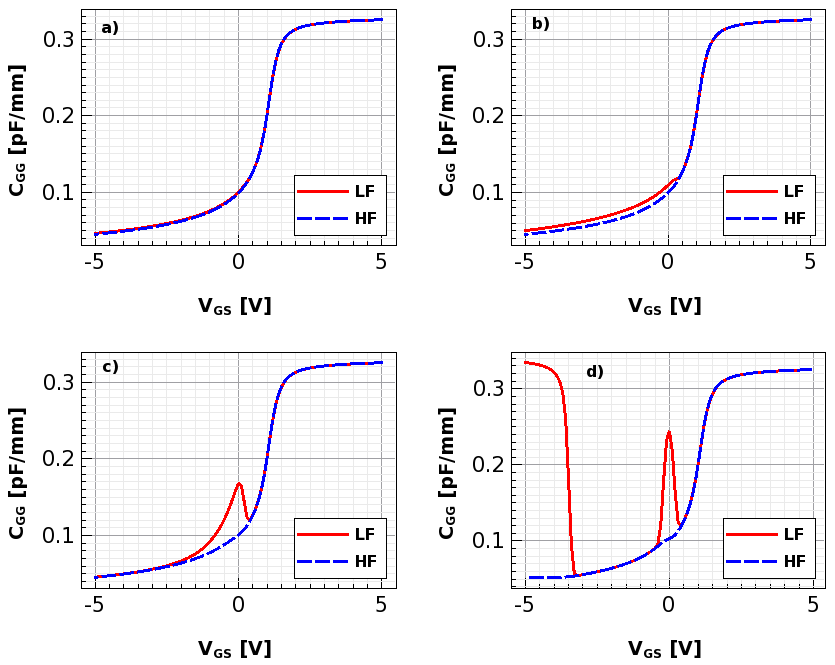
Figure 4. C–V characteristics of MOS device as obtained with transient and quasistationary simulation methods: (a) 10.0 V/s, (b) 1.0 V/s, (c) 0.1 V/s, and (d) quasistationary. (Click image for full-size view.)
Figure 4 shows the C–V characteristics of the device as obtained with the transient and quasistationary methods. There are two main aspects to consider from the characteristics:
- Deviation of low-frequency C–V (LF-CV) with respect to high-frequency C–V (HF-CV) at around Vg=0.0 V
- LF-CV at large negative gate bias conditions
For the first aspect, the deviation of LF-CV with respect to HF-CV increases as the ramp rate of the gate input slows down and is maximum when the quasistationary method is used. The deviation is mainly due to the partial response from the deep-level traps for different ramp rates. Figure 5 shows the electron trapped charge at the GaN–Oxide interface as obtained with different ramp rates and the quasistationary method. As the ramping time of the input gate signal increases, more electrons are de-trapped and the trapped electron density falls to a very low value.
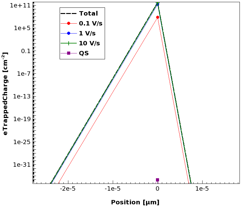
Figure 5. Electron trapped charge across the MOS device at Vg = -5 V for the corresponding simulation conditions shown in Figure 4. (Click image for full-size view.)
The second aspect is the accumulation of hole carriers at the GaN–Oxide interface for high negative bias conditions, which is reflected in the LF-CV characteristics with quasistationary simulations. Figure 6 shows the hole density at Vg= -5 V as obtained with transient and quasistationary simulations. The hole carriers response is instantaneous to the applied gate bias and shows up as a very high concentration at the GaN–Oxide interface. In experimental conditions, this is not expected since holes would take a very long time to be generated due to the wide bandgap of the GaN material.
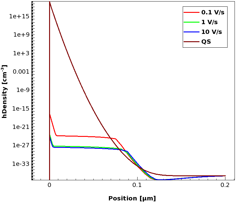
Figure 6. Hole density across the MOS device at Vg= -5 V for the corresponding simulation conditions shown in Figure 4. (Click image for full-size view.)
16.5.3.5 Summary
High-frequency and low-frequency C–V characteristics of an n-type GaN MOS device have been presented. The response of minority carriers and deep-level traps have been analyzed using the transient simulation method and compared against the quasistationary simulation approach.
Traps in wide-bandgap materials are very deep and do not respond to transients typically used to ramp up biases in DC experimental measurements. Using the quasistationary simulation method might not predict the correct device behavior in such conditions.
16.6 AlGaN-Specific Numeric Parameters
Simulations involving wide-bandgap materials are more prone to convergence problems due to the numeric challenges in performing floating-point operations with extremely large and extremely small numbers such as the concentrations of majority and minority carriers in wide-bandgap semiconductors.
Notably, III–nitride device simulations typically require a higher numeric precision to resolve low intrinsic carrier densities, caused by the wide bandgap of the materials. For this purpose, it is advisable to run III–nitride device simulations always in the ExtendedPrecision mode and to tighten the corresponding computation error controls moderately.
A proposed numeric parameter set for AlGaN HFET device simulations is:
Math {
  ExtendedPrecision
  #if [string match -nocase @aniso@ yes]
  TensorGridAniso(Aniso)
  #endif
  Method= Blocked
  SubMethod = ILS(set=27)
  ILSrc="
  set(26){
    iterative(gmres(100), tolrel=1e-16, tolunprec=1e-8, tolabs=0, maxit=200);
    preconditioning(ilut(1.0e-15,-1),left);
    ordering ( symmetric=nd, nonsymmetric=mpsilst );
    options( compact=yes, linscale=0, refineresidual=60, verbose=0);
  };
  set(27){
    iterative(gmres(100), tolrel=1e-10, tolunprec=1e-4, tolabs=0, maxit=200);
    preconditioning(ilut(1.0e-9,-1), right);
    ordering(symmetric=nd, nonsymmetric=mpsilst);
    options(compact=yes, linscale=0, refineresidual=10, verbose=0);
  };
  "
  Number_of_Threads= 4
  Digits=5
  Iterations=20
  Notdamped=30
  Transient= BE
  Traps(Damping=0)
  DirectCurrent
  ErrRef(electron) = 1e8
  ErrRef(hole)   = 1e8
  CDensityMin= 0
  RefDens_eGradQuasiFermi_ElectricField= 1e8
  RefDens_hGradQuasiFermi_ElectricField= 1e8
}
By default, ExtendedPrecision uses 80-bit accuracy for real numbers. In most cases, this is sufficient. For special cases, even higher precision settings are available. For details, refer to the Sentaurus™ Device User Guide.
The TensorGridAniso(Aniso) is the most robust approximation for the discretization of anisotropic tasks. It is an accurate approximation in the case of axis-aligned meshes if the anisotropy orientation coincides with the mesh orientation. For further discretization options of isotropic models such as mobility, see the discussion for SiC in Section 15.3.3 Material Parameter Anisotropy. For simulations with isotropic material properties, this Math setting can be omitted.
Transient=BE activates the backward Euler transient method instead of the default TRBDF method, which makes transient simulations run faster.
For the linear solver, use SubMethod=Super or SubMethod=ILS(set=26) with the dedicated solver parameter set, which is reliable and robust in the case of III–nitride HFET device simulations. The SUPER solver is good for small- or medium-sized 2D tasks. The ILS solver is more suitable for large 2D or 3D tasks due to its better parallel performance and lower memory requirements. Relaxed numeric settings for the ILS solver such as set(27) improves performance in many cases, but convergence might suffer.
For a detailed discussion about linear solvers and their various parameter settings, see Section 9.4 Linear Solvers.
Wide-bandgap device simulations usually require higher computational accuracy than common silicon device simulations. This is achieved by tightening the reference error control criteria from the default 1E10 to ErrRef(electron)=1E8 and ErrRef(hole)=1E8. In most cases, reducing these density references to even smaller values does not improve convergence in AlGaN/GaN HFETs.
For the Newton solver, typically, you should limit the number of nonlinear iterations to a small enough value, such as Iterations=20, and also avoid solution damping by specifying the number of nondamped iterations to be higher than the number of allowed Newton iterations (NotDamped=30). For a general discussion, see Section 6. Nonlinear System Newton Solver.
The trap model sometimes leads to convergence problems, especially at the beginning of a simulation when Sentaurus Device tries to find an initial solution. Often, you can solve this problem by changing the numeric damping of the trap charge in the nonlinear Poisson equation:
Math {
  Traps(Damping=0)
}
A value of 0 switches off damping. Large values increase damping (the default is 10). Depending on the particular example, increasing damping can improve or degrade convergence behavior. There are no guidelines regarding the optimal value of Damping.
For AlGaN/GaN HFETs, switching off trap charge damping is recommended if convergence is not an issue at the initial solution.
Occasionally, convergence problems can be attributed to the GradQuasiFermi driving force, particularly when the gradient of the quasi-Fermi level changes rapidly for small changes in the electron density. This is typically the case for regions with a small carrier density. In such cases, you can smoothly change the driving force from GradQuasiFermi to ElectricField for densities around or below a given carrier density. This transition density is set by RefDens_eGradQuasiFermi_ElectricField. A value of approximately 108 cm–3 is recommended for this type of simulation.
For details about this method, see Section 6.6 Improving Convergence in Low-Density or Low-Current Regions.
16.7 Application Example: p-Gate AlGaN HFET
This example demonstrates the Id–Vg simulation of a p-gate AlGaN/GaN HFET on a SiC substrate for various polarization models available in Sentaurus Device.
16.7.1 Project Configuration
The simulations are organized as a Sentaurus Workbench project (see Figure 7).
Figure 7. Organization of the p-gate AlGaN/GaN HFET project in Sentaurus Workbench. (Click image for full-size view.)
The project consists of Sentaurus Process and Sentaurus Device. The description of the process simulation part is provided in the Sentaurus Process module, Section 16. Special Focus: AlGaN Process Simulation.
This section focuses on the device simulation part.
16.7.2 Mesh Construction for Device Simulation
Requirements for mesh construction for process and device simulations are different. For device simulations, the mesh must be refined within the areas of spatial nonuniformities, such as large net doping profile gradients, material interfaces, and regions within the device, where some solution variables might experience large perturbations (areas with a strong electric field and large carrier impact ionization).
In this project, the mesh generation for the device simulation is performed within Sentaurus Process as the last step of the process flow.
HFETs typically do not contain doping profiles with strong gradients at locations other than interfaces. Similarly, carrier profiles exhibit large gradients only at heterointerfaces and in the space-charge region of Schottky contacts. Therefore, dedicated refinements are based on interface refinements to resolve such gradients:
refinebox name= waf_nuc                                 \
  interface.mat.pairs= "SiliconCarbide AlNnucleation"   \
  min.normal.size="1e-3"<um> normal.growth.ratio= 2
refinebox name= nuc_re1                                 \
  interface.mat.pairs= "AlNnucleation AlGaNrelax1"      \
  min.normal.size="1e-3"<um> normal.growth.ratio= 2
refinebox name= re1_re2                                 \
  interface.mat.pairs= "AlGaNrelax1    AlGaNrelax2"     \
  min.normal.size="1e-3"<um> normal.growth.ratio= 2
...
Maximum sizes for the lateral and vertical mesh spacings of the active part of the device are included in material-specific refinement boxes for the usual mesh refinements on net doping:
refinebox GaN adaptive refine.fields= {NetActive} \
  max.asinhdiff= {NetActive= 1.0} \
  refine.min.edge= {0.001 0.001} refine.max.edge= {0.25 0.15}
...
The device layer structure in a section under the gate is shown in Figure 8. Material layer interfaces are subject to mesh refinements to resolve abrupt changes of physical quantities. A part of the structure around the gate corner is magnified to demonstrate the accurate interface and junction mesh refinements (see Figure 9).
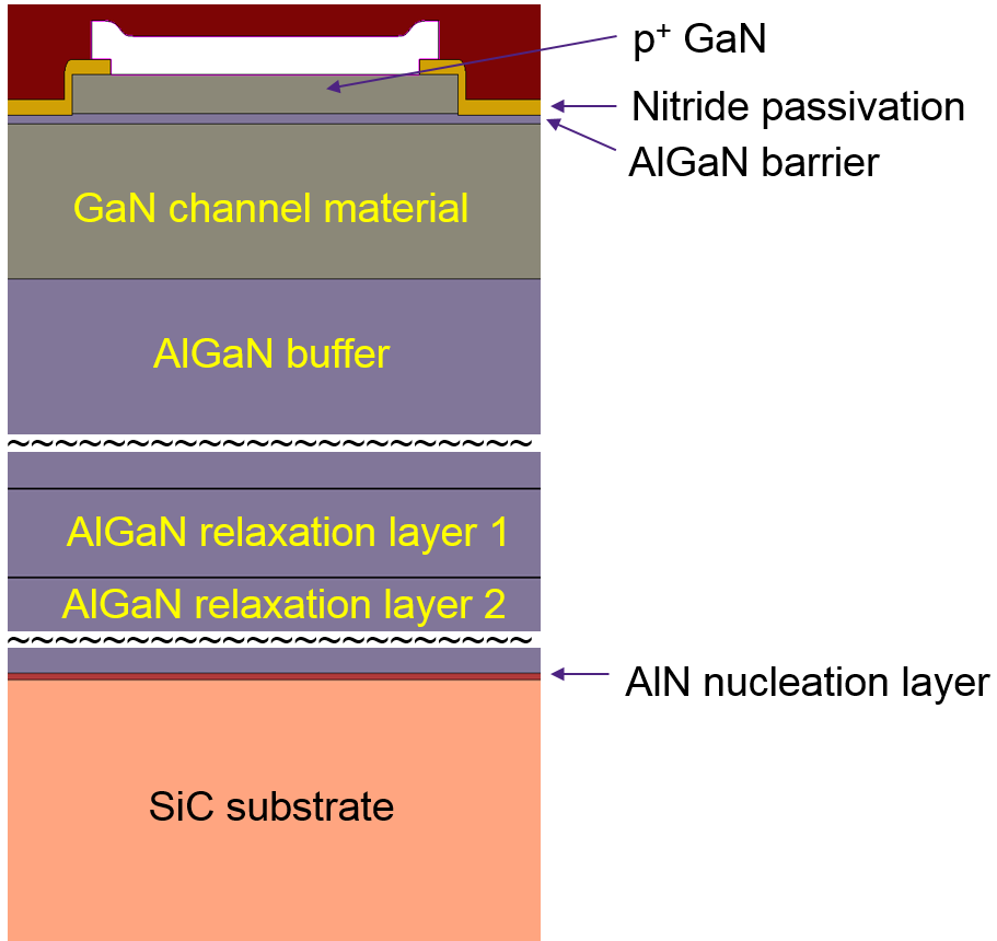
Figure 8. Device layer sequence in a window under the gate (layers are not shown to scale relative to each other). (Click image for full-size view.)
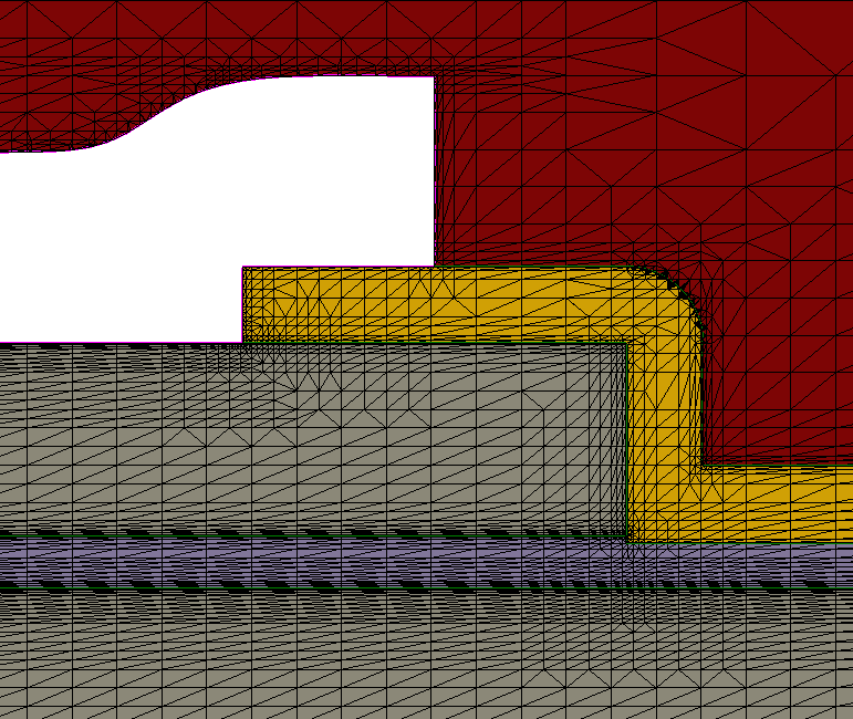
Figure 9. Mesh details in the vicinity of the gate corner, showing refinements at material interfaces and Schottky contacts. (Click image for full-size view.)
Click to view the primary file sprocess_fps.cmd.
16.7.3 Input Files for Device Simulation
In addition to the meshed device geometry, other input files are required for the stress/strain tensor if full polarization models will be used and PMIUserField profiles will be used for trap profile definitions. The stress distribution in the device is read from the Piezo file specified in the File section together with the files for the PMIUserFields:
File {
  Grid            = "@tdr@"
  Parameter       = "@parameter@"
  #if [string match -nocase "*@StrainFrom@*" "File_Stress"]
  Piezo           = "@tdr@"
  #endif
  PMIUserFields   = "@tdr@"
  Current         = "@plot@"
  Plot            = "@tdrdat@"
  Output          = "@log@"
}
16.7.4 Contacts
All contacts are implemented as Schottky contacts. For the source and drain contacts, this avoids nonphysical bending due to the Ohmic charge neutrality condition, where the contact crosses a heterointerface. To achieve Ohmic behavior, carriers are allowed to tunnel into the device with a reduced effective mass. For the p-gate contact, a standard Schottky contact is used and nonlocal tunneling is implemented along a nonlocal mesh.
The Electrode section reads:
Electrode {
  { name= "source" voltage=0.0 Workfunction= 4.3 Schottky}
  { name= "drain"  voltage=0.0 Workfunction= 4.3 Schottky}
  { name= "gate"   voltage=0.0 Workfunction= 5.8 Schottky}
}
Tunneling at the source and drain is activated for electrons, while holes are allowed to tunnel through the Schottky barrier into the highly p-doped gate GaN layer:
  eBarrierTunneling "sourceNLM"
  eBarrierTunneling "drainNLM"
  hBarrierTunneling "gateNLM"
The correspondingly named nonlocal meshes are defined in the Math section of the Sentaurus Device command file. For the source and drain, only tunneling into the channel is taken into account to mimic metal spikes contacting the channel directly:
  NonLocal "gateNLM" (
    electrode="gate"   Length= 20e-7  Digits= 4 EnergyResolution= 1e-3
  )
  NonLocal "sourceNLM"(
    electrode="source" Length= 30e-7  Digits= 4 EnergyResolution= 1e-3
    Direction=(0 1 0) MaxAngle=1 -EndPoint(Material="AlGaN")
  )
  NonLocal "drainNLM" (
    electrode="drain"  Length= 30e-7  Digits= 4 EnergyResolution= 1e-3
    Direction=(0 1 0) MaxAngle=1 -EndPoint(Material="AlGaN")
  )
16.7.5 Physics Settings
Currents and energy fluxes at an abrupt interface between two materials are better defined by thermionic interface conditions at the heterojunction. To activate such a thermionic current model for electrons and holes at all semiconductor interfaces, use the keyword Thermionic.
High carrier densities together with a moderate density-of-states require all simulations to be performed with Fermi statistics, which is activated with the Fermi keyword in the global Physics section.
Thermionic interface conditions specific to Fermi statistics are selected in the Thermionic parameter section of the parameter file by:
Thermionic { Formula= 1 }
Dopants in III–nitride materials have a relatively high ionization energy, especially magnesium, which acts as an acceptor and suffers from incomplete ionization. Incomplete ionization is activated using the keyword IncompleteIonization. An option is provided in this project to switch between complete and incomplete ionization:
  #if [string match -nocase @complete@ yes]
  IncompleteIonization
  #endif
Note that, in the parameter file, Si in AlGaN can form either a donor or an acceptor, depending on whether it sits on a group III or group V lattice site:
Material= "AlGaN" {
  Ionization {
    Species ("MagnesiumActiveConcentration") {
      E_0           =       0.15
      alpha         =       0
      g             =       4.0
      Xsec          =       1.0000e-12
    }
    Species ("pSiliconActiveConcentration") {
      E_0           =       0.1
      alpha         =       0
      g             =       4.0
      Xsec          =       1.0000e-12
    }
    Species ("nSiliconActiveConcentration") {
      E_0           =       0.05
      alpha         =       0
      g             =       2.0
      Xsec          =       1.0000e-12
    }
  }
}
AlGaN must be added to the list of materials, for which magnesium acts as an acceptor. For an updated list of materials, use a project-specific datexcodes.txt file. The corresponding entry reads:
MagnesiumConcentration, MagnesiumChemicalConcentration {
    label     = "total (chemical) Magnesium concentration"
    symbol    = "MgTotal"
    unit      = "cm^-3"
    factor    = 1.0e+12
    precision = 4
    interpol  = log
    material  = All
    property("floops") = "MgActive"
    doping    = acceptor (
                     active = MagnesiumActiveConcentration
                     ionized = MagnesiumMinusConcentration
                     material = AlN, GaN, AlGaN, InGaAs, InGaAsP, InP
                 )
}
For low-field mobilities, the Masetti doping-dependent mobility model is used. It is activated by the mobility flag DopingDependence. The corresponding GaN, AlN, and AlGaN parameters are provided in the default parameters from the MaterialDB parameters set. For the high-field saturation model, you use the standard Canali model for stability reasons.
  Mobility (
    DopingDependence
    HighFieldSaturation(GradQuasiFermi)
  )
As an alternative, a negative differential mobility is implemented, namely, TransferredElectronEffect2. However, this is rarely used due to convergence issues inherent in negative differential mobility models.
The Sentaurus Workbench parameter aniso is provided for this project and acts as a switch to treat the dielectric properties isotropically or anisotropically. Anisotropic treatment of the permittivity for the Poisson equation is activated by:
  #if [string match -nocase @aniso@ yes]
  Aniso (
    Poisson
    direction(SimulationSystem)= xAxis
  )
  #endif
For III–nitride materials with direct band gap, radiative recombination will contribute as a fast recombination mechanism. This is activated by the option Radiative in the list of recombination mechanisms in the global Physics section:
  Recombination (
    SRH
    Radiative
  )
For the SiC wafer, radiative recombination is deactivated by:
Physics (Region= "wafer") {
  Recombination (-Radiative)
}
The Sentaurus Workbench parameter StrainFrom is provided to switch between the full and the simplified strain model as well as the full stress model. The corresponding commands are:
  #if [string match -nocase @StrainFrom@ Model]
  Piezoelectric_Polarization(strain)
  #elif [string match -nocase @StrainFrom@ File]
  Piezo( Strain= LoadFromFile )
  Piezoelectric_Polarization(strain)
  #elif [string match -nocase @StrainFrom@ Stress]
  Piezoelectric_Polarization(stress)
  #endif
Traps are implemented as passivating species at the GaN–nitride and AlGaN–nitride interfaces. At interfaces deeper into the layer stack, traps are assumed to form and they partially capture polarization-induced charges. Bulk traps are used throughout the deeper layers, assuming that trap densities decrease towards the channel layer. The corresponding interface and bulk trap settings are:
Physics (RegionInterface= "pgate/passivation_left") {
  Piezoelectric_Polarization(Activation=1.0)
  Traps (( Donor Level fromCondBand EnergyMid= 0.4
    Conc= 3e13 eXsection=1e-14  hXsection=1e-14 )
  )
}

Physics (RegionInterface= "pgate/passivation_right") {
  Piezoelectric_Polarization(Activation=1.0)
  Traps (( Donor Level fromCondBand EnergyMid= 0.4
    Conc= 3e13 eXsection=1e-14 hXsection=1e-14 )
  )
}

Physics (RegionInterface= "alganbarrier/passivation_left") {
  Traps (( Donor Level fromCondBand EnergyMid= 0.4
    Conc= 3e13 eXsection=1e-14 hXsection=1e-14)
  )
}

Physics (RegionInterface= "alganbarrier/passivation_right") {
  Traps (( Donor Level fromCondBand EnergyMid= 0.4
    Conc= 3e13 eXsection=1e-14 hXsection=1e-14)
  )
}

Physics (RegionInterface= "buffer/channel") {
  Traps (( Donor Level fromMidBandGap EnergyMid= 0
    Conc= 2e11 eXsection=1e-14 hXsection=1e-14)
  )
}

Physics (RegionInterface= "relax2/buffer") {
...
Physics (RegionInterface= "nucleation/relax1") {
  Piezoelectric_Polarization(Activation=0.2)
}
All simulations are performed as slow transient simulations. This helps to achieve convergence especially in the case of floating regions within the device. Polarization charges at the interfaces of buried layers frequently induce such floating regions. Therefore, transient solutions are recommended for most AlGaN/GaN devices with complex layer structures. For the drain ramp given here, the default physical ramp time is 1 s:
  Transient (
    InitialStep=0.01 MinStep=1.0e-4 maxstep=0.1
    goal { name= drain voltage=@Vds@ }
  ) { coupled { Poisson Electron Hole } }
Click to view the primary file IdVg_des.cmd.
16.7.6 Simulation Results
Figure 10 shows the transfer characteristics at two different drain voltages. All three polarization models result in almost the same drain currents. The small differences between the simplified model and the full models result from the inhomogeneous stress distribution around the gate corner, induced by strain relaxation after etching of the p-gate layer.
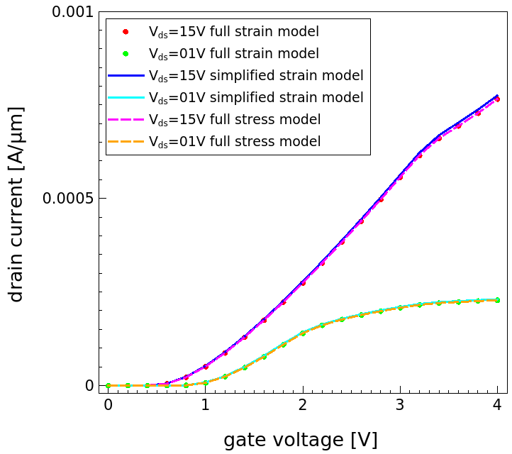
Figure 10. Transfer characteristics for the available stress models. (Click image for full-size view.)
Figure 11 shows the StressZZ component of the stress tensor, focusing on the gate corner. The simplified strain model assumes homogeneous strain throughout the barrier layer.
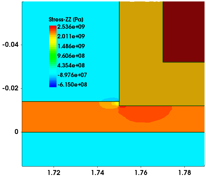
Figure 11. Inhomogeneous stress distribution showing the zz component of the stress tensor, focusing on the gate corner. (Click image for full-size view.)
Figure 12 shows a comparison of the transfer characteristics for the device with isotropic and anisotropic dielectric properties at two different drain voltages. The primary effect of dielectric anisotropy is a threshold voltage shift.
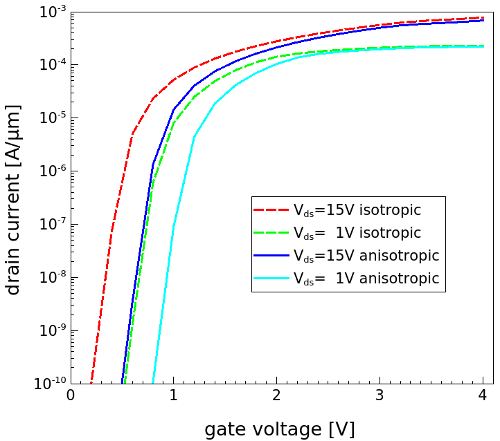
Figure 12. Transfer characteristics with and without dielectric anisotropy. (Click image for full-size view.)
This threshold voltage shift originates from the higher permittivity along the c-axis of the crystal, compared to the isotropic value. Note that the isotropic model uses the same parameter value as the value in the plane normal to the anisotropic direction. If the higher permittivity of the anisotropy direction is used for the isotropic model, the results are very close to each other as expected (see Figure 13).
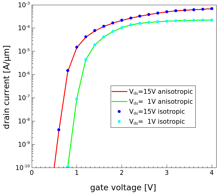
Figure 13. Transfer characteristics with and without dielectric anisotropy. The isotropic permittivity model uses the value of the dielectric constant along the c-axis in this comparison. (Click image for full-size view.)
16.8 Application Example: GaN p-i-n Diode
This example demonstrates the simulation of a GaN material–based p-i-n diode under forward and reverse bias conditions. The electrical characteristics of the p-i-n diode are determined, accounting for the relevant GaN material physics, including piezoelectric polarization, material anisotropy, interface charge trapping, incomplete dopant ionization, and radiative recombination. The simulation is performed in slow transient.
16.8.1 Project Configuration
The simulations are organized as a Sentaurus Workbench project (see Figure 14).
Figure 14. Organization of GaN p-i-n diode project in Sentaurus Workbench. (Click image for full-size view.)
The GaN p-i-n model structure is built with Sentaurus Structure Editor. There are two tool instances of Sentaurus Device: the first tool instance, sd_fdiv, simulates the forward bias characteristics, and the second tool instance, sd_rviv, simulates the reverse bias characteristics until breakdown.
16.8.2 Device Structure Generation
Sentaurus Structure Editor defines the model geometry, adds doping profiles to the model, defines contact regions, and finally builds the mesh. Basic Scheme commands are used to create the p, i, and n regions of the p-i-n diode. The corresponding regions are doped at constant doping levels of 1019, 1015, and 1019 cm–3.
Click to view the Sentaurus Structure Editor primary file sde_dvs.cmd.
For a detailed introduction to Sentaurus Structure Editor, see the Sentaurus Structure Editor module.
Figure 15 shows the meshed device structure. A part of the structure at the GaN–Nitride interface is magnified to demonstrate the accurate interface mesh refinements.
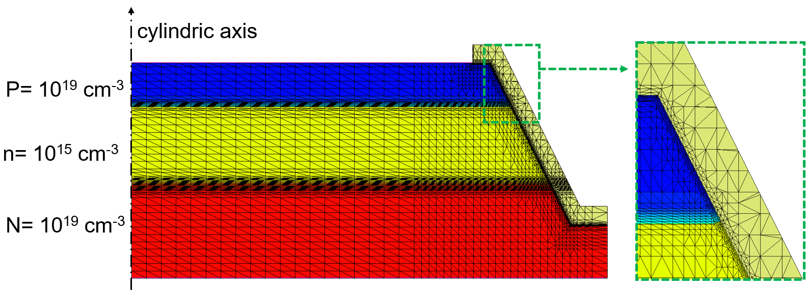
Figure 15. GaN diode geometry with mesh details at the beveled isolation interface. (Click image for full-size view.)
16.8.3 Meshing Strategy
The meshing strategy follows the requirement of the proper resolution of areas with large net doping profile gradients, material interfaces, and regions within the device, where some solution variables might experience large perturbations. To that end, the following mesh refinements are made:
- A global mesh for the entire structure
- An automatic doping refinement
- An extra refinement at the N-n transition
- Coarse axis-aligned mesh refinement at the GaN–Nitride interface
- Fine boundary-conforming mesh refinement at the GaN–Nitride interface
The corresponding Sentaurus Structure Editor commands for Sentaurus Mesh are:
;--- meshing ------------------------------------------------------------------;
(define xmin (sde:min-x (get-body-list)))
(define xmax (sde:max-x (get-body-list)))
(define ymin (sde:min-y (get-body-list)))
(define ymax (sde:max-y (get-body-list)))

(sdedr:define-refeval-window       "Ref.Win.Global"
  "Rectangle" (position xmin ymin 0) (position xmax ymax 0))
(sdedr:define-refinement-size      "Ref.Def.Global"
  0.05 0.1 0.005 0.005 )
(sdedr:define-refinement-function  "Ref.Def.Global"
  "DopingConcentration" "MaxTransDiff" 1)
(sdedr:define-refinement-function  "Ref.Def.Global"
  "MaxLenInt" "GaN" "Nitride" 0.015 1.2)
(sdedr:define-refinement-placement "Ref.Pla.Global"
  "Ref.Def.Global" (list "window" "Ref.Win.Global" ) )

(sdedr:define-refeval-window "Ref.Win.ni"
  "Rectangle"  (position (- xi 0.05) 0 0) (position (+ xi 0.01) radius_sub 0))
(sdedr:define-refinement-size "Ref.Def.ni"
  0.01 0.1 1 0.001 0.001 1 )
(sdedr:define-refinement-placement "Ref.Pla.ni"
  "Ref.Def.ni" (list "window" "Ref.Win.ni" ) )

(sdedr:offset-interface "material" "GaN" "Nitride" "hlocal" 0.002 "factor" 1.2)
(sdedr:offset-interface "material" "Nitride" "GaN" "hlocal" 0.005 "factor" 1.4)
(sdedr:offset-block "material" "GaN" "maxlevel" 4)
(sdedr:offset-block "material" "Nitride" "maxlevel" 2)

(sde:build-mesh "" "n@node@")
16.8.4 Device Simulation
Input files required for device simulation and output files to be saved after device simulation are specified in the File section.
File {
  * input files
  Grid      = "@tdr@"
  Parameters= "@parameter@"

  * output files
  Plot      = "@tdrdat@"
  Current   = "@plot@"
  Output    = "@log@"
}
Electrical boundary conditions at predefined electrodes are specifed in the Electrode section. The following code excerpt defines "anode" as a contact in series with a resistor of 1e12 Ω, with the 0 V external voltage applied to the resistor. The "cathode" is defined as a contact set at 0 V voltage.
Electrode {
  { Name= "anode"   Voltage= 0 Resist=1e7 }
  { Name= "cathode" Voltage= 0}
}
The device simulation for the p-i-n diode is performed invoking the following models in the Physics sections:
- Transport model: Drift-diffusion
- Carrier statistics: Fermi
- Bandgap model: Default, Bennett–Wilson model
- Bandgap narrowing: Off
- Generation–recombination: SRH, Auger, radiative, and avalanche generation
- Mobility: Doping dependence (Masetti model), high-field saturation (Caughey–Thomas model), and transverse field mobility degradation (Lombardi model)
- Piezoelectric polarization model: Strain-based piezo model
- Anisotropy: On
- IncompleteIonization: On
- Traps: Donor type at GaN–Nitride interface
The global Physics section reads:
Physics {

  Temperature=  300.00
  Fermi
  Piezoelectric_Polarization(strain) * strain-based piezo model
  DefaultParametersFromFile
  EffectiveIntrinsicDensity(NoBandgapNarrowing)

  * bulk generation/recombination
  Recombination (
    SRH
    Auger
    Radiative
    * Avalanche generation model activation with driving force specification
    Avalanche(vanOverstraeten)
  )

  * Carrier mobility
  Mobility (
    DopingDependence(Masetti)
    HighFieldSaturation(CaugheyThomas)
    * Transverse field mobility degradation
    Enormal(Lombardi) * Lombardi interface degradation mobility model
  )

  IncompleteIonization
  Aniso (
    Poisson * Global aniso permittivity model activation
    direction(SimulationSystem)= (1 0 0)
  )
}
The interface-specific Physics section reads:
Physics (MaterialInterface= "GaN/Nitride") {
  * Interface trap specification
  Traps (
    (Donor           * trap type
      Conc=3e13       * trap density, 1/cm^2
      Level           * trap energetic distribution
      FromMidBandGap  * reference energy position
      EnergyMid=0.36  * central energy position of energetic distribution
      eXsection=1e-30 * trap cross-section for electrons, cm^2
      hXsection=1e-14 * trap cross-section for holes, cm^2
    )
  )
}
The simulation is performed in slow transient using the following commands. The "cathode" is set to be ramped to -1e4 V and a current break criterion is defined. The simulation stops when the "cathode" current exceeds 1e-5 A.
Solve {
  Coupled (Iterations=500) { Poisson }
  Coupled (Iterations=100) { Poisson Hole }
  Coupled (Iterations=100) { Poisson Electron Hole }

  Transient (
    InitialStep= 1e-10 MinStep= 1e-15 MaxStep= 1e-2
    Increment= 1.4
    Goal{ Name= "anode" Voltage= -1e4 }
    BreakCriteria { Current (Contact = "cathode" absval = 1e-5) }
  ) { Coupled { Poisson Electron Hole } }
}
Click to view the primary file sd_rviv_des.cmd.
16.8.5 Visualization of Results
Figure 16 shows the forward bias and reverse bias current–voltage characteristics of the GaN p-i-n diode.
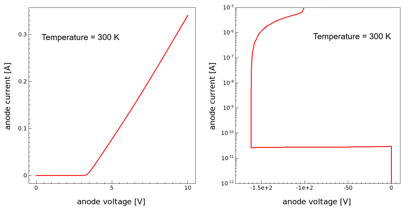
Figure 16. (Left) Forward bias and (right) reverse bias current–voltage characteristics of GaN p-i-n diode. (Click image for full-size view.)
The two Sentaurus Visual tool instances, plot_fdiv and plot_rviv next to the Sentaurus Device tools, plot the forward bias and reverse bias characteristics. In addition, plot_rviv estimates the breakdown voltage (Sentaurus Workbench parameter, BV) and the simulation time (Sentaurus Workbench parameter, tBV) corresponding to the breakdown. Figure 17 shows the impact ionization (contour bands) and the current potential (contour lines) distributions at breakdown.
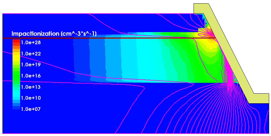
Figure 17. Impact ionization (contour bands) and the current potential (contour lines) distributions in breakdown. (Click image for full-size view.)
16.9 Relevant Application Notes
- App. 1
- Optimization of GaN MISFET and DC Boost Converter Circuit, available from Applications_Library/Power/BoostConverter_GaN-SiC/ BoostConverter_MixedMode.
- App. 2
- Simulation of Polarization-Induced Effects at AlGaN–GaN Heterointerfaces, available from Applications_Library/Power/GaN/GaN_AlGaN_Polarization.
- App. 3
- Simulation of Normally On GaN HEMT Device by Using Calculated Polarization Charges, available from Applications_Library/Power/GaN/GaN_AlGaN_Polz_Calculated.
- App. 4
- Simulation of Normally Off AlGaN/GaN HFET With p-Type GaN Gate and AlGaN Buffer, available from Applications_Library/Power/GaN/HFET_pGate_GaN.
- App. 5
- Process and Device Simulations of GaN HFET Devices, available from Applications_Library/Power/GaN/GaN_Processing.
- App. 6
- Simulation of Vertical GaN Devices: Trench-Gate MOSFET and Diodes, available from Applications_Library/Power/GaN/GaN_Vertical_MOSFET_SW.
- App. 7
- Using Carrier Statistics to Model 2D Electron Gas at AlGaN–GaN Interface, available from Applications_Library/Power/GaN/GaN_HEMT_FermiStat.
- App. 8
- Simulation of Leakage due to Tunneling in p-GaN Schottky Barriers, available from Applications_Library/Power/GaN/pGate_Schottky_1D.
- App. 9
- Simulation of Leakage due to Trap-Assisted Tunneling in p-GaN Schottky Barriers, available from Applications_Library/Power/GaN/pGate_Schottky_TAT_1D.
- App. 10
- Two-Dimensional Simulation of Corner-Rounding Effects in p-GaN Schottky Barriers, available from Applications_Library/Power/GaN/pGate_Schottky_2D.
- App. 11
- Simulation of Leakage Through AlGaN Barriers in Typical p-GaN Gate HEMT Layer Structures, available from Applications_Library/Power/GaN/ pGate_Barrier_TAT_1D.
- App. 12
- Two-Dimensional Simulation of Leakage in Source-Side Stack of p-GaN Gate HEMTs, available from Applications_Library/Power/GaN/pGate_Leakage.
- App. 13
- Two-Dimensional Device Simulation of p-GaN Gate HEMTs, available from Applications_Library/Power/GaN/pGate_HEMT.
- App. 14
- Modeling of Self-Heating Effects in GaN HFETs, available from Applications_Library/Power/GaN/GaN_HFET_SH.
- App. 15
- Modeling and Simulation of Trapping Effects in p-GaN Gate HEMT Gate Injection Transistor, available from Applications_Library/Power/GaN/pGate_HEMT_CC.
- App. 16
- Three-Dimensional Simulation of GaN Fin-HEMT, available from Applications_Library/Power/GaN/GaN_Fin-HEMT.
- App. 17
- Sentaurus Technology Template: Simulation of DC Characteristics of a GaN-Based HFET, available from Applications_Library/Hetero/HFET_GaN_DC.
Copyright © 2022 Synopsys, Inc. All rights reserved.