
Sentaurus Process
15. Special Focus: SiC Process Simulation
15.1 Overview
15.2 Substrate Definition
15.3 Ion Implantation
15.4 Dopant Diffusion and Activation
15.5 Oxidation
15.6 Application Example: SiC PiN Diode
Objectives
- To demonstrate how to perform process simulations with SiC substrates.
15.1 Overview
Sentaurus Process can simulate all process steps on silicon carbide (SiC) substrates. Its capabilities include:
- Definition of different SiC polytype substrates and crystal orientations
- Ion implantation
- Diffusion
- Oxidation
This section discusses special settings required to perform SiC process simulations.
15.2 Substrate Definition
This section describes how to define the substrate.
15.2.1 Polytype Specification
Unlike silicon, SiC has different crystal structures called polytypes. Sentaurus Process supports simulations with polytypes 2H, 4H, 6H, and 3C. The default polytype is 4H. To set a different polytype, use one of the following commands:
- set2H-SiC
- set6H-SiC
- set3C-SiC
If the substrate is 4H-SiC, you should invoke Advanced Calibration using the command:
AdvancedCalibration 4H-SiC
This command will set not only the polytypes but also the correct parameters such as the lattice constants.
15.2.2 Wafer and Flat Orientations
The next step is to choose the wafer orientation and the flat orientation. For the 3C (cubic) polytype, this process is similar to silicon. For the hexagonal polytypes, the hexagonal crystal system must be taken into account.
In a hexagonal crystal, four Miller indices are used to define a direction: a1, a2, a3, and c. However, a1, a2, and a3 depend on each other with the relationship: a1 + a2 + a3 = 0. Therefore, it is sufficient to use only three of the four Miller indices to determine any direction.
Sentaurus Process uses only a1, a2, and c to define a direction. For example, the direction [1120] is specified in Sentaurus Process as {1 1 0}, omitting the third Miller index.
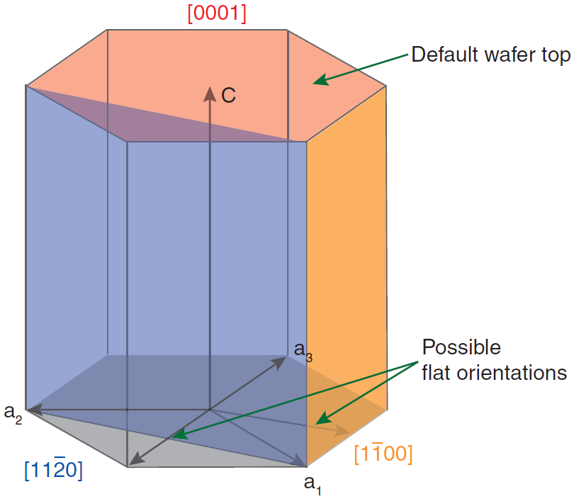
Figure 1. Crystal orientations in a hexagonal SiC polytype. (Click image for full-size view.)
To specify the wafer and flat orientations, use the init command:
init wafer.orient= {a1 a2 c} notch.direction= {a1 a2 c}
The default wafer orientation is [0001], which is specified as wafer.orient= {0 0 1}. Most SiC wafers are grown in this orientation.
In Sentaurus Process, possible flat orientations for such wafers are [1100] specified as notch.direction= {1 -1 0} or [1120] specified as notch.direction= {1 1 0}.
Hexagonal SiC lattices with [0001] wafer orientation consist of alternating layers of Si and C in the [0001] direction. As a convention, if the wafer orientation is specified as [0001], this means that the topmost layer is a Si layer. If the topmost layer is a C layer, by convention such wafers are defined to have a wafer orientation of [0001].
Such wafers can be specified in Sentaurus Process with wafer.orient= {0 0 -1}. Choosing the proper topmost layer is important for an accurate oxidation rate.
15.2.3 Wafer Miscut
SiC wafers are usually cut at an angle of 3.5–8.5°, not exactly at crystal directions. To specify this miscut, use the miscut.angle and miscut.toward arguments of the init command:
init miscut.tilt= 4 miscut.toward= {1 1 0}
The miscut.tilt argument is the angle by which the actual wafer normal is tilted with respect to wafer.orient. The miscut.toward argument specifies the direction towards which the wafer normal is tilted. This is usually the wafer flat direction. Most wafers are miscut towards the [1120] orientation (flat orientation), that is, miscut.toward= {1 1 0}.
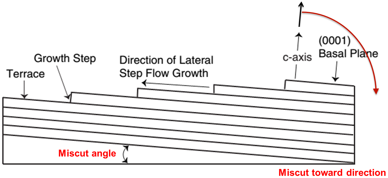
Figure 2. Definition of miscut angle. (Click image for full-size view.)
15.3 Ion Implantation
This section discusses ion implantation.
15.3.1 Performing MC Ion Implantation Into SiC
Sentaurus Process supports only Monte Carlo (MC) implantation into SiC. There are no analytic tables. MC implantation can be performed with:
implant <species> dose=<n> energy=<n> tilt=<n> particles=<n> sentaurus.mc
The number of particles specified is per 50 nm of the wafer width, not the total number of particles. In general, at least 2000 particles must be implanted to obtain reasonable statistics. For complicated geometries, as many as 10 000 particles might be needed.
Sentaurus MC implantation can be slow, so it is advisable to run it using parallel processing with:
math numThreadsMC=<i>
15.3.2 Calibration Range of MC Ion Implantation Into SiC
Extensive calibration of MC implantation parameters has been performed for B, Al, and N implantation into 4H-SiC with wafer orientation [0001], including a small miscut. To use these calibrated parameters, invoke Advanced Calibration:
AdvancedCalibration 4H-SiC
The calibration is valid in the following dose or energy ranges:
- Aluminum:
- Most implantation energies in the range between 20 keV and 5 MeV.
- Most doses in the range between 1013 cm–2 and 5x1014 cm–-2.
- Boron:
- Energies between 10 keV and 5.8 MeV.
- Most doses in the range between 1013 cm–2 and 5x1014 cm–2.
- Nitrogen:
- Energies between 10 keV and 5.8 MeV.
- Most doses in the range between 1014 cm–2 and 2x1015 cm–2.
15.3.3 Performing Additional Calibration
To calibrate MC implantation models into other SiC polytypes or polytypes of other species into 4H-SiC, you can adjust the following parameters:
- LSS.pre: Nonlocal electronic stopping power.
- nloc.pre: Local electronic stopping power pre-exponential.
- nloc.exp: Local electronic stopping power exponent.
- surv.rat: Dynamic annealing.
These parameters can be changed from their Advanced Calibration values by creating a procedure called UserImpPreProcess:
proc UserImpPreProcess { Species Energy Dose Tilt Rotation Slice Mode } {
     if {$Species=="<dopant>"} {
  pdbSet SiliconCarbide $Species <parameter> <value>
     }
}
The effect of these parameters on the implantation profile is illustrated in Figure 3 to Figure 5.
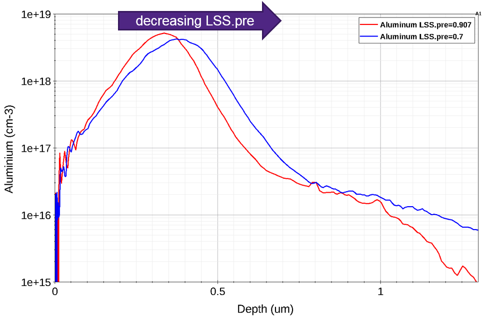
Figure 3. The parameter LSS.pre calibrates the implantation depth. (Click image for full-size view.)
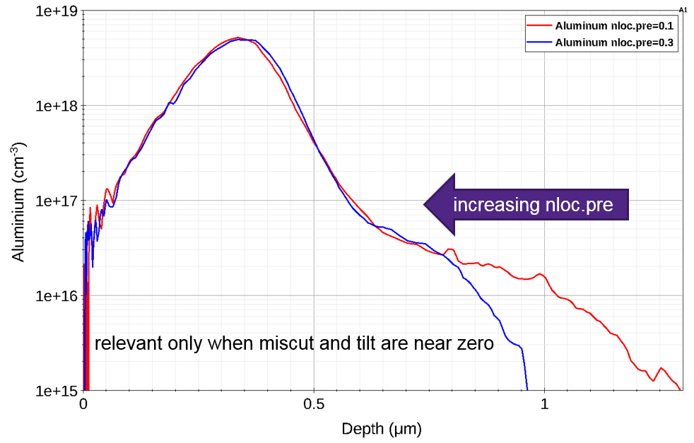
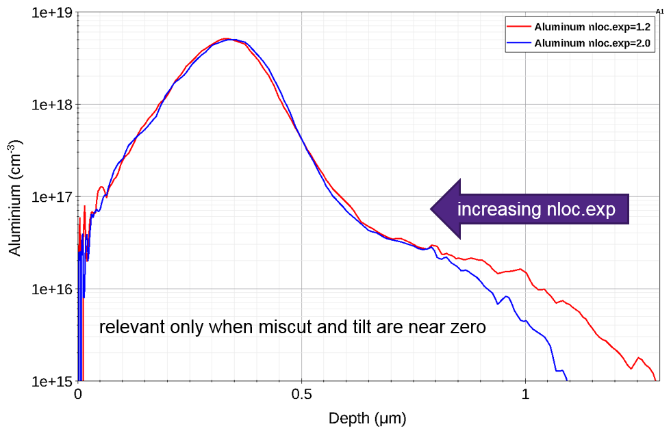
Figure 4. The parameters (top) nloc.pre and (bottom) nloc.exp calibrate the amount of channeling for zero-tilt implantations. (Click images for full-size views.)
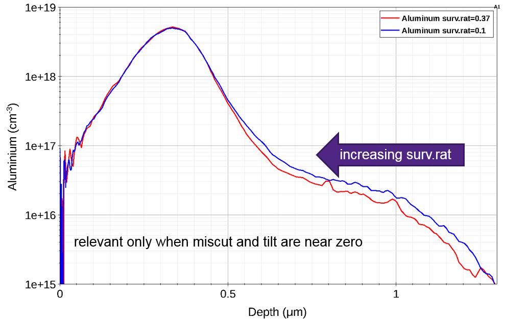
Figure 5. The parameter surv.rat calibrates the damage accumulation rate, which can affect the amount of channeling. (Click image for full-size view.)
15.4 Dopant Diffusion and Activation
Dopants diffuse in SiC using interstitial and vacancy mechanisms like in silicon. Two types of interstitial (IntSilicon, IntCarbon) and two types of vacancy (VacSilicon, VacCarbon) are present.
Since little data exists for interstitial and vacancy components of dopant diffusivities in SiC, macroscopic diffusivity values have been used to develop a diffusion model with constant diffusivity for Al, B, N, and P in 4H-SiC. Literature values for macroscopic diffusivities have been used without any calibration. The constant diffusivity model does not take any of the following effects into account:
- Fermi-level dependency
- Oxidation enhancement or retardation
- Transient-enhanced diffusion
By default, Sentaurus Process uses the Solid model for dopant activation in SiC, which assumes dopants activate and deactivate to solid solubility values instantly, and this can result in dopants being inactive at the end of the flow. Therefore, you should use Advanced Calibration for SiC, which sets the activation model to Transient, that is, activation and deactivation with a time constant.
In addition, Advanced Calibration for SiC increases the maximum annealing temperature, so anneals at high temperature (>1400°C) can be performed.
15.5 Oxidation
The mechanism for oxidation of SiC is similar to oxidation of silicon substrates, except that, in addition to SiO2, CO and CO2 are formed as by-products of the reaction. Such carbon oxides diffuse to the surface of the SiO2 layer and evaporate.
Sentaurus Process provides a calibrated parameter set for the following oxidation conditions:
- [0001] surface (Si terminated) for oxidants O2 and H2O
- [0001] surface (C terminated) for oxidants O2 and H2O
- [1120] surface for oxidant O2
The orientation of the surface is determined automatically from the crystal orientation set by the init command and the orientation of the surface within the simulation domain. No intervention by users is needed.
15.6 Application Example: SiC PiN Diode
This section presents a SiC process simulation using a PiN diode, which can be found in the project Applications_Library/GettingStarted/sdevice/4H-SiC_PiN.
See Section 15. Special Focus: 4H-SiC PiN Device Breakdown Simulation for a description of the device simulation part of the same example.
The concept of the simulated device in this project and its geometry follows the publication of R. Pérez et al., "Planar Edge Termination Design and Technology Considerations for 1.7-kV 4H-SiC PiN Diodes," IEEE Transactions on Electron Devices, vol. 52, no. 10, pp. 2309–2316, 2005.
Click to view the command file sprocess_fps.cmd.
In the first part of the process flow, the substrate definition is performed. The wafer is 4H-SiC, with a wafer orientation of [0001], a flat orientation of [1120], and a 4° miscut towards the wafer flat:
line x location= @epithick@     spacing= 0.5	tag= xtop
line x location= @<epithick+5>@ spacing= 1.0 tag= xbottom
line y location= 0       		tag= yleft
line y location= @width@    		tag= yright

region SiliconCarbide xlo= xtop xhi= xbottom ylo= yleft yhi= yright
init field= Nitrogen concentration= 1e19 !DelayFullD \
	wafer.orient= {0 0 1} notch.direction= {1 1 0} \
	miscut.tilt= @miscut@ miscut.toward= {1 1 0}

AdvancedCalibration 4H-SiC
In addition, a 10 μm epitaxial layer with a concentration of 9x1015 cm–3 is grown:
deposit SiliconCarbide anisotropic thickness= @epithick@ species= Nitrogen \
	concentration= 9e15
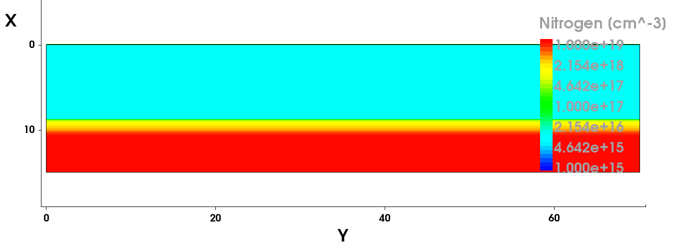
Figure 6. Structure after epitaxy. (Click image for full-size view.)
Then, a series of mask and implantation steps are performed for the JTE1, JTE2, and anode regions. The implantation masks differ depending on whether JTE1 and JTE2 overlap or not. Only the anode is shown here:
mask name= ANODE left= 0 right= @awidth@
photo mask= ANODE thickness= 3

implant Aluminum dose= 4e13 energy= 20 tilt= 7 rotation= 0 \
	sentaurus.mc particles= @particles@ info= 1
implant Aluminum dose= 2e14 energy= 80 tilt= 7 rotation= 0 \
	sentaurus.mc particles= @particles@ info= 1
implant Aluminum dose= 2e14 energy= 160 tilt= 7 rotation= 0 \
	sentaurus.mc particles= @particles@ info= 1

strip Photoresist
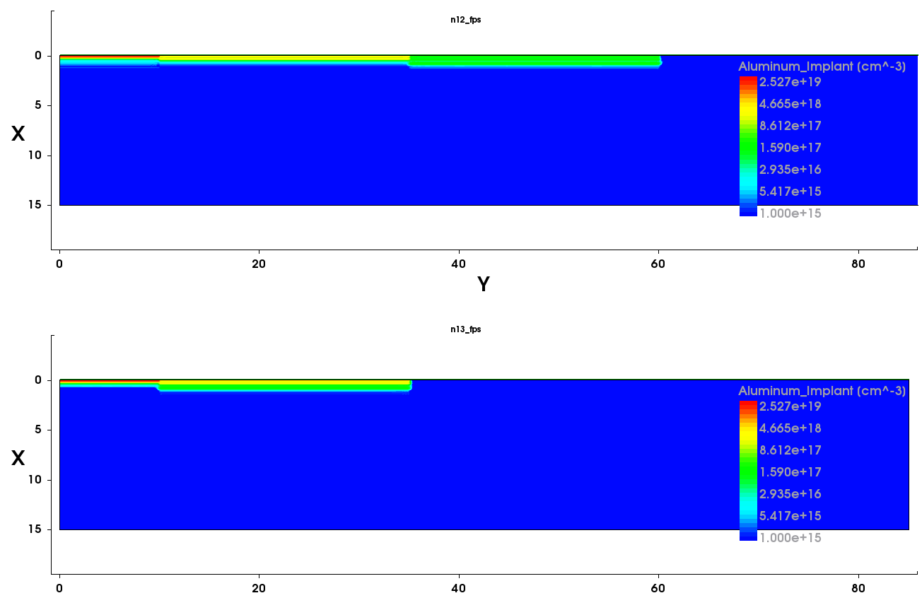
Figure 7. Structure after implantations: JTE1 and JTE2 do not overlap. (Click image for full-size view.)
After that, the wafer is annealed at 1700°C for 30 minutes, followed by oxidation in H2O ambient:
# Activation
diffuse time= 30 temperature= 1700

# Passivation oxide
diffuse time= 120 temperature= 1200 H2O
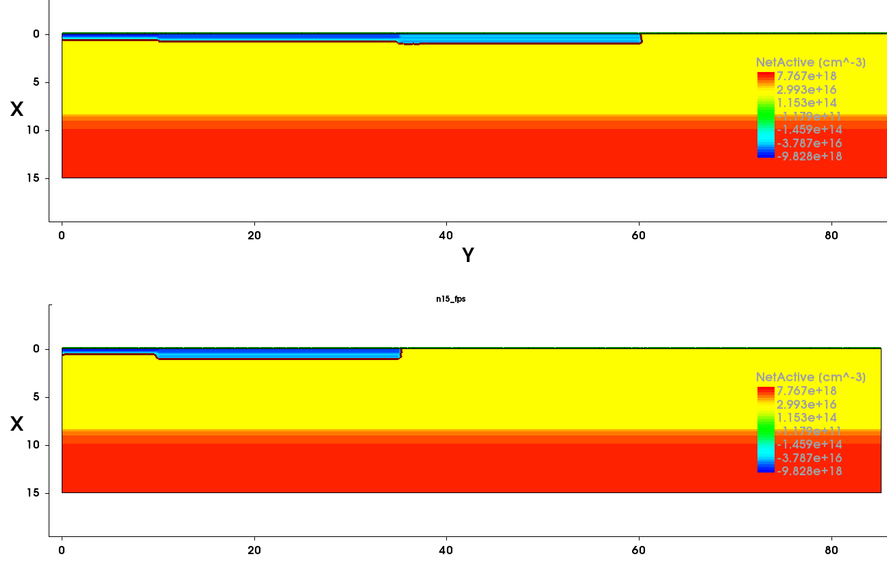
Figure 8. Structure after anneal and oxidation: JTE1 and JTE2 do not overlap. (Click image for full-size view.)
Then, the contact hole is etched and the anode metal is deposited:
deposit oxide anisotropic thickness= 0.4

mask name= ANODE left= 0 right= @awidth@
photo mask= ANODE thickness= 1
etch Oxide anisotropic thickness= 0.6
strip Photoresist
deposit Aluminum type= fill coord= 0
Finally, the device is meshed for device simulations and the contacts are defined. See the Sentaurus Device module, Section 15.5.2 Mesh Construction for Device Simulation for details about this step.
Copyright © 2022 Synopsys, Inc. All rights reserved.