
Sentaurus Device
5. Unified Interface for Optical Generation Calculation
5.1 Integrating Optics Into Sentaurus Device
5.2 Calculating the Wavelength-Dependent Reflection Using TMM
5.3 Calculating the Illuminated I–V Curve of a Simple Solar Cell Using TMM
5.4 Calculating the Angular-Dependent Reflection Using Raytracing
5.5 Calculating the White Light Photocurrent of a 3D Photodiode Using Raytracing
5.6 Calculating Quantum Efficiency Versus Frequency Using Optical AC Analysis
Objectives
- To learn how optics are integrated into Sentaurus Device.
- To understand how absorbed photons are converted to charged carriers.
- To demonstrate wavelength ramps and how to use a spectrum for illumination.
- To demonstrate how to perform optical calculations both standalone and coupled to electronics.
- To demonstrate how to perform optical AC analysis.
5.1 Integrating Optics Into Sentaurus Device
Sentaurus Device allows you to calculate the optical charge generation using different solvers, such as the transfer matrix method (TMM), raytracing, OptBeam (Beer's law), and the beam propagation method (BPM), or to load external generation profiles, for example, calculated by Sentaurus Device Electromagnetic Wave Solver.
Regardless of the chosen optical solver, the Sentaurus Device setup for optics and the procedure for coupling optical generation to electronics are identical (see Figure 1).
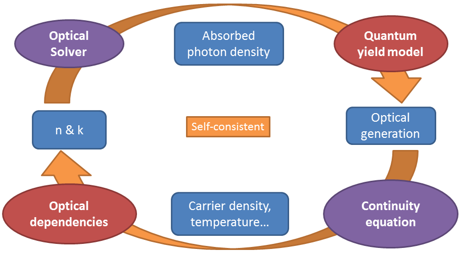
Figure 1. Simulation flow of optical device simulation. (Click image for full-size view.)
For example, for a region in the simulation domain, you can specify the refractive index (n) and the extinction coefficient (k) using different complex refractive index models, such as constant, wavelength dependent, temperature dependent, carrier dependent, or user defined. Based on the n&k values, the selected optical solver calculates the absorbed photon density, which at each vertex gives the number of absorbed photons per volume and seconds.
After choosing a suitable quantum yield model, you define how the absorbed photon density is converted to the optical generation rate. The complexity of the quantum yield model ranges from a simplistic model (unity) that assumes that each absorbed photon generates one electron–hole pair, to complex models (effectiveAbsorption) that account for free carrier absorption. A physical model interface is available to specify even more complicated user-defined models.
Then, the optical generation is added to the continuity equation. Therefore, all other equations can be solved self-consistently with that optical generation. Depending on the chosen complex refractive index model, n&k values might be dependent on temperature or carrier density. In that case, the above-described steps are repeated until convergence is achieved. However, in most cases, for passive devices, the influence of temperature and carrier density on n&k values is weak, such that the cycle is evaluated only once.
5.2 Calculating the Wavelength-Dependent Reflection Using TMM
This section explains the fundamental features of the unified interface for optical generation computation. As an example, the wavelength-dependent reflection of a planar silicon substrate, coated with a single silicon nitride (SiN) layer, is calculated using the transfer matrix method (TMM). The calculation is purely optical; no electrical equations are solved. Therefore, the optical generation is not of interest here.
The complete project can be investigated from within Sentaurus Workbench in the directory Applications_Library/GettingStarted/sdevice/opto/tmm-spectral-reflection.
All settings for optics are defined in an Optics(...) section inside the global Physics section. The settings inside the Optics section, in turn, can be categorized as common to all solvers such as ComplexRefractiveIndex(...), OpticalGeneration(...), and Excitation(...) or as a solver-specific section such as OpticalSolver(...).
In the following sections, you will work through all the specific settings of the example.
5.2.1 ComplexRefractiveIndex Section
The appropriate model for the n&k values must be specified in the Sentaurus Device command file.
Click to view the command file sdevice_des.cmd.
In this case, for SiN, you want to use a constant refractive index of n=2.74 with no absorption (k=0) and, for silicon, wavelength-dependent tabulated values for n (real part of the refractive index) and k (imaginary part of the refractive index) will be used, which are activated in the command file with the following line:
ComplexRefractiveIndex (WavelengthDep(Real Imag))
The values themselves are defined in the parameter file sdevice.par of Sentaurus Device in the corresponding ComplexRefractiveIndex sections.
The keyword Formula switches the source from where the wavelength-dependent values are read:
- Formula=0 uses a second-order polynomial for the wavelength dependency specified by the coefficients *_lambda.
- Formula=1 uses the NumericalTable(...) values.
- Formula=2 reads in the values from an external file (specified by NumericalTable=...).
- Formula=3 reads in the values from the TableODB section. This option is used for backward compatibility reasons.
The constant refractive index for SiN uses Formula=0:
Material = "Nitride" {
  ComplexRefractiveIndex {
    n_0	= 2.74	# [1]
    k_0	= 0.0	# [1]
    Formula = 0
  }
}
However, for silicon, tabulated values are used:
Material = "Silicon" {
  ComplexRefractiveIndex {
    n_0	= 3.45	# [1]
    k_0	= 0.0	# [1]
    Cn_temp	= 2.0000e-04	# [K^-1]
    Cn_carr	= 1	# [1]
    Ck_carr	= 0.0000e+00 ,	0.0000e+00	# [cm^2]
    Gamma_k_carr	= 1 ,	1	# [1]
    Cn_gain	= 0.0000e+00	# [1]
    Npar	= 1.0000e+18	# [cm^-3]
    Formula = 1
    NumericalTable (
      # wavelength [um]  n [1] k [1];
      0.1908	0.84	2.73;
      0.1984	0.968	2.89;
      ...
    )
  }
}
It is important to note that only these coefficients are used, for which a model has been activated in the command file. For example, although the temperature dependency coefficient Cn_temp is specified, it is not used here because TemperatureDep is omitted in the ComplexRefractiveIndex section of the command file.
5.2.2 OpticalGeneration Section
The OpticalGeneration section defines how the optical generation is calculated and from which source the profiles are used. The available options are:
- SetConstant uses a constant optical generation over the entire region. It also can be used in a region or material Physics section to set a constant optical generation for a particular region only.
- ReadFromFile reads optical generation from an external file.
- ComputeFromSpectrum uses an illumination spectrum where, typically, the optical generation is calculated for a list of wavelengths with a particular intensity, and the profiles are summed to a white light generation.
- ComputeFromMonochromaticSource uses a monochromatic light source.
The last option is the appropriate source in this case, since you want to sweep through a monochromatic light source to extract the reflection for each wavelength:
OpticalGeneration ( ComputeFromMonochromaticSource )
5.2.3 Excitation Section
In the Excitation section, everything concerning illumination including light direction, polarization, wavelength, and illumination window is set:
    Excitation (
      Wavelength = @wstart@  *[um]
      theta = 0 * angle of incidence from +y to +x axis
                * 0 points in +y direction, 90 in +x direction.
      Intensity = 0.1 *[W/cm2]
      Polarization = 0.5 * TE, TM or a number P 0..1 where P = I_TE/I_tot
      Window(
        Origin=(0,-@dSiN@)
        Line(x1=0 x2=1)
      )
    ) * end excitation
The wavelength is set to the Sentaurus Workbench parameter @wstart@ with a value of 0.3 μm and is used as the start wavelength here. Ramping the wavelength can be performed in the Solve section later.
The excitation direction is defined with respect to the global coordinate system (GCS) given by the grid. It is set with theta=0 to point into the +y-direction (see Figure 6, left). The second angle for setting the excitation direction (phi) is not used in two dimensions. The illumination intensity is arbitrary here as the reflection is a relative value. The polarization defines the part of the TE polarized light and is set to 0.5, which means that both TE and TM polarization are present in equal parts.
An illumination window defines the area where light falls onto the device. It is defined with the Window(...) command. For convenience, the plane of the illumination window is specified in a local coordinate system (LCS), which you can shift and rotate with respect to the GCS (see Figure 2). Actually, the LCS is a plane (x', y') in three dimensions. In two dimensions, the LCS is a line (x').
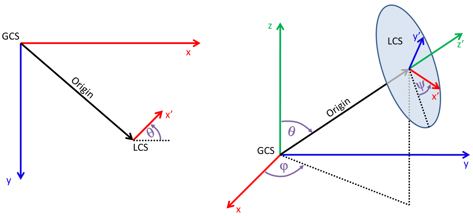
Figure 2. Definition of the LCS with respect to the GCS in (left) two dimensions and (right) three dimensions. (Click image for full-size view.)
The offset of the LCS origin with respect to the GCS is controlled with the keyword Origin=(<x>, <y>). By default, Origin=(0, 0), that is, the LCS is equal to the GCS.
In this example, the SiN layer of the structure starts at y=-@dSiN@, where the Sentaurus Workbench parameter @dSiN@ defines the SiN layer thickness and has a value of 0.075. Since light will fall on top of the SiN layer, the origin of the LCS must be shifted up by @dSiN@. This is achieved by setting Origin=(0,-@dSiN@).
The Line command defines the start point and the endpoint of the illumination window in the LCS. Here, the entire width of the structure from x1=0 to x2=1 is illuminated (see Figure 3).
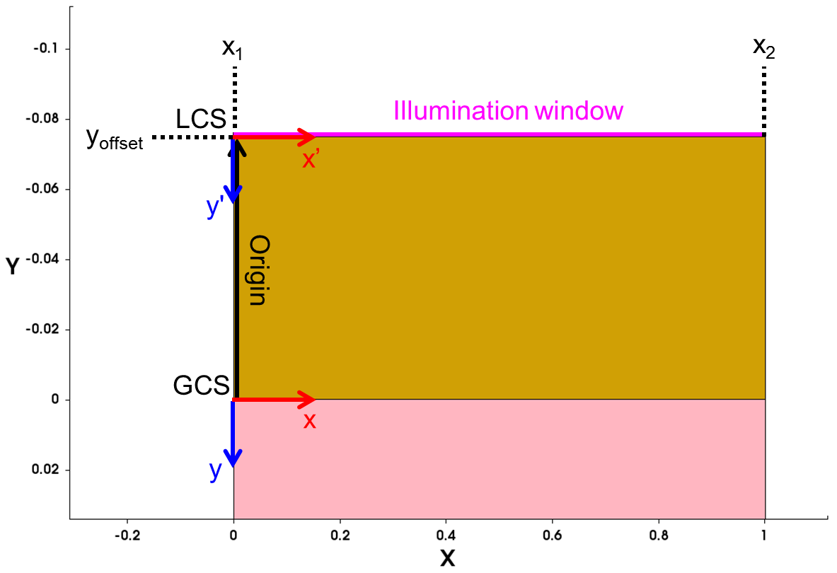
Figure 3. Defining the illumination window in a 2D structure. (Click image for full-size view.)
The excitation direction is defined with respect to the GCS and is independent of the illumination window orientation.
5.2.4 OpticalSolver Section
The solver and solver-specific settings are defined in the OpticalSolver section. Only one solver is allowed.
In this example, the TMM solver is used:
      TMM (
        LayerStackExtraction(
          Medium(
            Location = Bottom
            Material = "Silicon"
          )
        ) * end LayerStack
      ) * end TMM
As the TMM solver is a 1D solver, you must instruct Sentaurus Device from where it must extract the 1D layer stack. This is done using the LayerStackExtraction command, which by default creates an extraction line in the center of the illumination window and perpendicular to the illumination window, in the same direction as light falls through the illumination window. In this example, the layer stack extraction starts at (0.5,-@dSiN@) and points downwards in the +y-direction.
HINT When setting up the simulation, always check the illumination window settings in the log file:
IlluminationWindow("unnamed_0"):
Origin: (0.0000e+00, -7.5000e-02, 0.0000e+00)
XDirection: (1, 0.0000e+00, 0.0000e+00)
LayerStackExtraction("unnamed_0"):
Position of starting point: (0.5, -7.5000e-02, 0.0000e+00)
Direction of extraction line: (-0.0000e+00, 1, 0.0000e+00)
as well as the extracted layer stack itself:
Multilayer Structure:
---------------------
Layer | Thickness [um] |      n |         k | alpha [cm^-1] |  mean abs [1]
    0                0   1.0000   0.000e+00       0.000e+00       0.000e+00
    1            0.075   2.1542   0.000e+00       0.000e+00       0.000e+00
    2                2   5.0042   4.161e+00       1.743e+06       4.137e-01
    3                0   5.0042   4.161e+00       1.743e+06       0.000e+00
Later in this example, you will want to neglect any reflection from the rear side, assuming a very thick (semi-infinite) silicon substrate. This can be achieved with the Medium command, by explicitly specifying the semi-infinite region at the bottom of the TMM stack as silicon.
5.2.5 Solve Section
In this example, you want to solve only optics without any other electrical equation. This is achieved using the keyword Optics.
In addition, optics will be solved for several wavelengths. In this case, it should be computed for the wavelength range @wstart@ to @wend@, using @wsteps@ steps. As any parameter defined in the Optics section can be ramped in the Quasistationary statement, the following lines will do this:
  Quasistationary (
    DoZero
    InitialStep = @<1./wsteps>@ MaxStep = @<1./wsteps>@ Minstep = @<1./wsteps>@
    Goal { modelParameter="Wavelength" value=@wend@ }
  ) {
    Optics
  }
The step size is fixed by setting InitialStep, MaxStep, and MinStep to 1/@wsteps@. The start wavelength @wstart@ is specified in the Excitation section, while the end wavelength @wend@ is specified in the Goal statement.
5.2.6 Plotting the Results
Different solvers can output different results. In the case of the TMM solver, the reflection, the transmission, and the total absorption are directly available in the .plt file.
To plot against wavelength, the wavelength must be added to the .plt file. This is done in the Sentaurus Device command file by adding Wavelength to the CurrentPlot section:
CurrentPlot{
  ModelParameter="Wavelength"
}
With this, the reflection curve can be created easily with the following lines in Sentaurus Visual:
set n @previous@
set proj "@plot@"
set varWavelength "Device=,File=CommandFile/Physics,DefaultRegionPhysics,"
set varWavelength "${varWavelength}ModelParameter=Optics/Excitation/Wavelength"
set varR "LayerStack(unnamed_0) R_Total"
set ds($n) [load_file_datasets $proj]
create_curve -name R($n) -dataset $ds($n) -axisX $varWavelength -axisY $varR
Click to view the complete command file svisual_vis.tcl.
Finally, clicking the Run Selected Visualizer Nodes Together toolbar button generates the required reflection versus wavelength plot (compare Section 2.7 Visualizing Selected Nodes Together). The minimum of the reflection has shifted as the thickness of the SiN coating changes (see Figure 4).
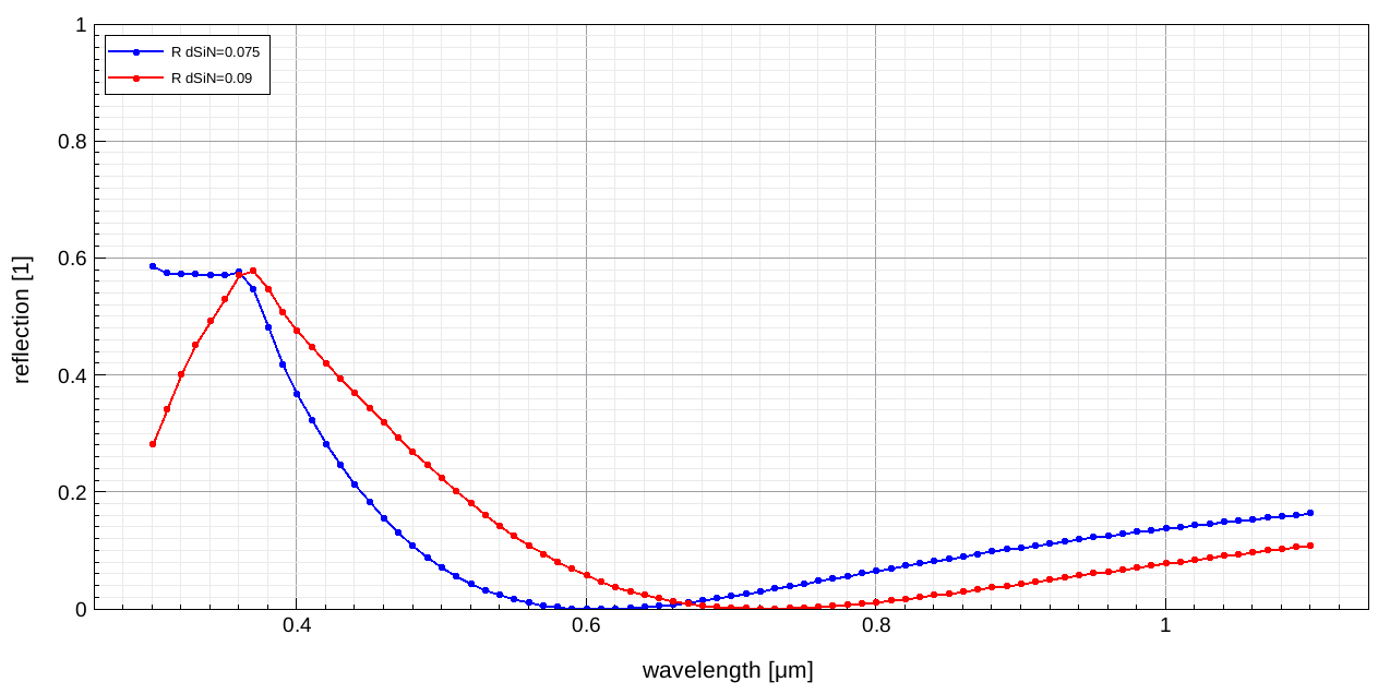
Figure 4. Reflection versus wavelength for two different SiN thicknesses using the TMM solver. (Click image for full-size view.)
5.3 Calculating the Illuminated I–V Curve of a Simple Solar Cell Using TMM
This section discusses combined optical and electrical equations, and addresses spectral illumination. As an example, the I–V curve of a simple 2D solar cell illuminated with the standard solar spectrum AM1.5g is calculated using the TMM solver. The characteristic I–V solar cell parameters such as short circuit current, open circuit voltage, and efficiency are extracted in a subsequent Sentaurus Visual script.
The complete project can be investigated from within Sentaurus Workbench in the directory Applications_Library/GettingStarted/sdevice/opto/tmm-light-iv.
Similarly as in Section 5.2 Calculating the Wavelength-Dependent Reflection Using TMM, a planar silicon substrate with a single antireflective coating is used. However, in addition, doping is added to form a pn junction and an electrical front-finger grid is applied, which brings some 2D effects into the simulation (see Figure 5).
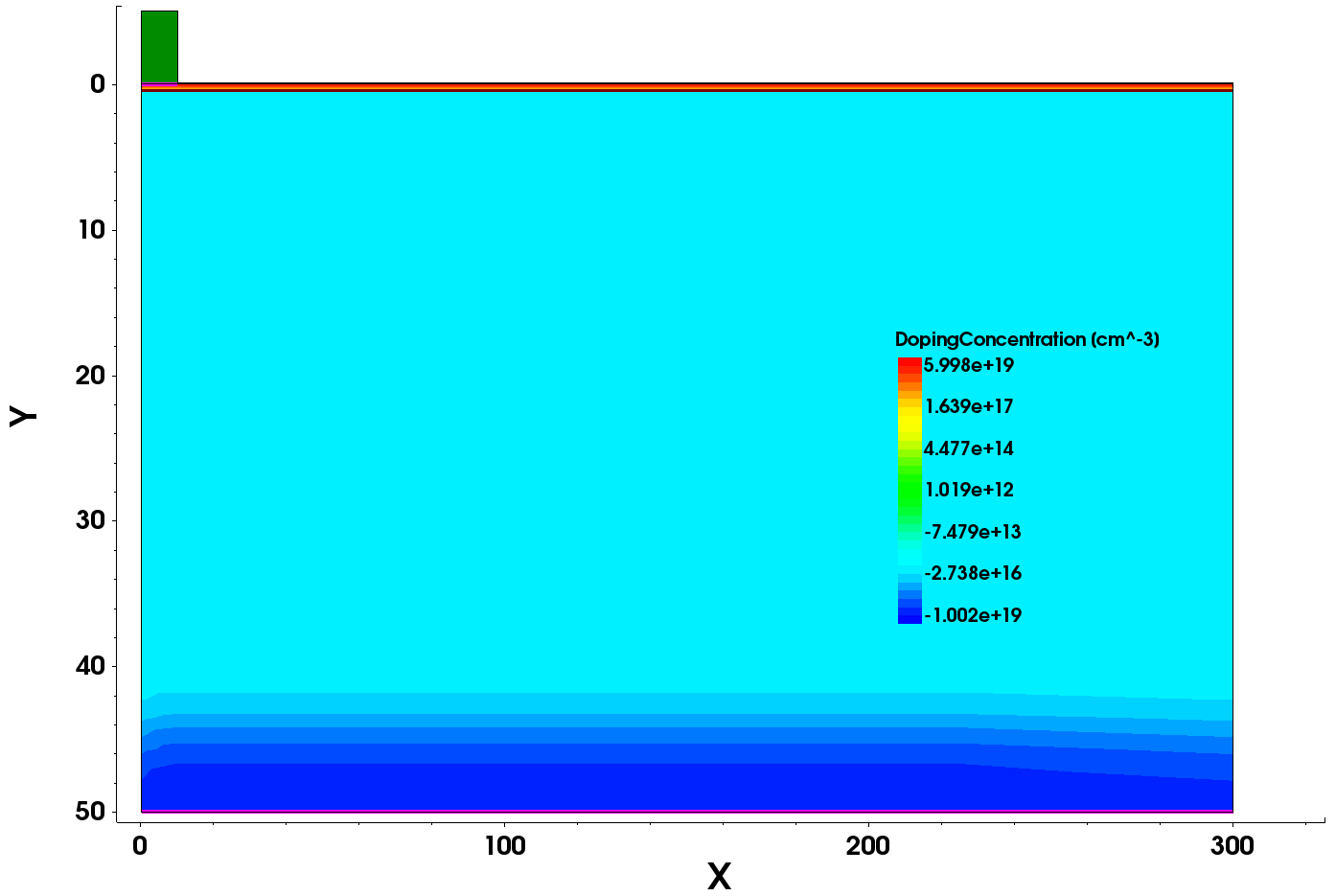
Figure 5. Simple 2D silicon solar cell structure. (Click image for full-size view.)
If you compare the Excitation section of the Sentaurus Device command file to the previous project tmm-spectral-reflection, you will notice that there is no explicit Origin keyword to shift the illumination window to the top of the structure:
    Excitation (
      fromTop
      Window (
        * origin is not required, as fromTop automatically shifts the
        * illumination window to the top of the structure.
        # Origin = (0,-0.075)
        Line(x1=!(puts -nonewline $wfront)! x2=!(puts -nonewline $wtot)!)
    ...))
This is due to the keyword fromTop, which automatically determines the top of the structure and sets the origin of the illumination window accordingly. It also takes into account the coordinate system orientation of the grid and its dimension, and sets the orientation of the illumination window as well as the excitation angles theta and phi accordingly. The keyword fromTop also assumes that the light is incident, perpendicular from the top, and covers the entire device.
You can customize the excitation further, by specifying additional settings. Here, for example, the Line command reduces the illumination window to cover only the silicon region without metallization. You can double-check the settings in the log file:
Optics Excitation: fromTop option activated
  DFISE coordinate system
  Theta = 0.0000e+00 (auto set)
  PolarizationAngle = 0.0000e+00 (auto set)
Optics Excitation: fromTop option activated for Window unnamed_0
  DFISE coordinate system
  Origin = ( 0.0000e+00 -5.0001e+00 )  (auto set)
  XDirection = ( 1 0.0000e+00 )  (auto set)
  Line: X1 = (10)  (set by user),  X2 = (3.0000e+02)  (set by user)
If you want to illuminate your structure from the bottom, you can use fromBottom.
5.3.1 Interpolating the 1D Absorbed Photon Density Profile to the Device Grid
The TMM solver calculates the absorbed photon density (APD) on a 1D grid, defined by the LayerStackExtraction statement (see Section 5.2.4 OpticalSolver Section). However, the electrical simulation usually is a 2D or 3D domain. Therefore, some interpolation from the 1D optical grid to the higher dimensional electrical grid is necessary. In the following, you will focus on the TMM solver using a 2D electrical grid; however, the considerations are also valid for 3D electrical grids.
When the TMM solver is used for very thick layers. such as the substrate region or buffer layer, for a wavelength where the device becomes transparent and where, in addition, some reflection occurs underneath, standing wave patterns can form. That is, the APD oscillates with a period in the submicron range (wavelength/(2n)). This oscillation typically cannot be resolved by the electrical grid. Consequently, during the interpolation, when Sentaurus Device looks up the APD value on the fine 1D TMM grid, a slight change in the vertex position on the coarse mesh can move from a maximum to a minimum on the fine grid, resulting in very large interpolation errors.
To circumvent this issue, Sentaurus Device can control how the intensity – the APD is proportional to the intensity – in the TMM solver is calculated, using the keyword IntensityPattern:
    OpticalSolver (
      TMM (
        LayerStackExtraction ()
        IntensityPattern = Envelope
      ) *end TMM
    )	* end OpticalSolver
By default IntensityPattern=StandingWave, the forward- and backward-propagating optical fields are summed, and then the result is squared to obtain the intensity. However, it can be shown that, for thick layers, it is accurate to first square the forward- and backward-propagating fields and then sum them (IntensityPattern=Envelope).The latter approach results in a very smooth intensity profile and, therefore, a smooth APD, which is more insensitive to coarse mesh interpolation.
Use Envelope whenever you cannot resolve the standing wave pattern and your layer thickness is at least 3 times the wavelength.
A second interpolation issue can arise due to lateral discretization of the electrical grid. This issue concerns not only the TMM solver but also any 1D optical solvers, such as OptBeam and fromFile using 1D profiles.
By default, Sentaurus Device simply checks whether or not each vertex lies inside the projected illumination window. If a vertex is inside, it is assigned the full APD value; otherwise, 0. Consequently, the accuracy of the photogenerated current crucially depends on the lateral alignment of mesh vertices with respect to the illumination window.
You can improve the accuracy of the integrated APD due to misalignment of the illumination window and mesh vertices using the WeightedAPDIntegration option, which can be specified in the Excitation(Window(...)) section.
Activating this feature, Sentaurus Device calculates a target-integrated APD value by integrating the 1D APD profile on the very fine TMM grid and multiplying it by the illumination window area. In a second step, fringe vertices of the 2D device grid, that is, vertices that have neighbor vertices outside the projected illumination window, are scaled such that the integral of the APD on the 2D device grid corresponds to the target value.
For the given example, the default interpolation scheme results in a deviation of the photogeneration current of 0.07 mA/cm2. For more complicated structures or for moving windows, the deviation might be much larger. For this reason, it is recommended to use the WeightedAPDIntegration option for any 1D optical solver.
5.3.2 Computing Optical Generation From Spectrum
In contrast to the previous examples, now you will illuminate the device with a complete spectrum. The spectrum is defined in a separate file and is set in the File section:
File {
  IlluminationSpectrum = "@pwd@/am15g.txt"
}
The spectrum file usually consists of a list of wavelength and intensity pairs:
# AM 1.5 global solar spectrum according to ASTM IEC904-3
# intensity = 0.1 W/cm2
# integration has to be performed according to Sum(y_i)
wavelength [um] intensity [W*cm^-2]
+3.0750000e-01 +1.2986361e-05
+3.1250000e-01 +3.7582516e-05
+3.1750000e-01 +7.2282062e-05
+3.2250000e-01 +1.0708551e-04
...
In Sentaurus Device, a spectrum file has a much more general meaning than a list of wavelengths and intensities. It basically defines an intensity depending on one or several other parameters. Therefore, it can consist of an arbitrary number of columns plus one intensity column. Examples would be a wavelength-dependent and angular-dependent spectrum, or an angular intensity distribution in three dimensions depending on two angles.
The units of the entries can be changed in the header line so that you can easily read in data in other units without having to rescale the data. For example, to read in wavelengths in nanometers and intensity in mW/m2, use:
wavelength [nm] intensity [mW*m^-2]
To activate spectral illumination, you must specify ComputeFromSpectrum in the OpticalGeneration(...) section. Sentaurus Device then computes the optical generation profiles for all wavelengths using the corresponding intensities and sums them to form a single profile, the white light optical generation profile.
When summing the different optical generation profiles, it is important to use an adequate quantum yield model. In this case, the StepFunction(EffectiveBandgap) model has been chosen, which assumes that each absorbed photon with an energy greater than the effective band gap creates an electron–hole pair. Otherwise, no carriers are generated.
Consequently, as you are interested only in the wavelength range that produces charge carriers, you can omit the computation of wavelengths greater than the effective band gap. To select the spectral range of interest, use the following Select statement in the ComputeFromSpectrum section:
      ComputeFromSpectrum(
        Select(
          Parameter=("Wavelength")
          Condition="$Wavelength <= 1.2"
        )
        keepSpectralData
      ) * end ComputeFromSpectrum
Here, Parameter defines the list of column names from the spectrum file that are used in the Select statement. Condition is a string forming a valid Tcl expression, where identifiers preceded by a dollar sign ($) refer to the respective column in the spectrum file. Therefore, the above condition selects all entries from the spectrum file with a wavelength smaller than or equal to 1.2 μm.
Identifiers without a preceding dollar sign refer to a Sentaurus Device parameter.
Usually, during a ComputeFromSpectrum calculation, the spectral data (the solution for each single spectrum entry) is lost. However, specifying the keyword keepSpectralData saves all the spectral data, that is, the reflection, transmission, absorption, intensity,and spatial APD for each wavelength into the file specified with SpectralPlot in the File section.
File {
  SpectralPlot         = "n@node@_spec"
}
Click to view the complete command file sdevice_des.cmd.
Open the file n*_spec.tdr and select the AbsorbedPhotonDensity-* entries, one after another, to see how the absorption depth increases with increasing wavelength.
In addition, open the file n*_spec.plt and create a reflection curve by plotting LayerStack(Unnamed_0) R_Total against wavelength or the spectrum itself by plotting intensity against wavelength.
For a ComputeFromSpectrum calculation, the reflection values in the file specified by the Current keyword (not the file specified by the SpectralPlot keyword) correspond to the spectral-weighted reflection.
Investigate the Sentaurus Visual script to see how it uses the spectrum plot to visualize the reflection curve.
Click to view the complete command file svisual_vis.tcl.
5.4 Calculating the Angular-Dependent Reflection Using Raytracing
In this section, the basics of using the raytracer are explained with a simple 2D example that calculates the reflectance of a planar semi-infinite silicon substrate for different angles of incidence. The calculation is purely optical; no electrical equations are solved. Therefore, optical generation is of no interest here.
The complete project can be investigated from within Sentaurus Workbench in the directory Applications_Library/GettingStarted/sdevice/opto/rt-angular-r.
5.4.1 Boundary Conditions at Interfaces
In Sentaurus Device, an interface is defined as the face (3D) or the edge (2D) of two adjacent regions. For each interface, where boundary conditions (BCs) other than the default Fresnel BC are required, you must define the BC as to how the raytracer will propagate any impinging ray. As a consequence, care must be taken when setting up the device structure, such that all interfaces of special interest actually have two adjacent regions.
Click to view the complete command file sde_dvs.cmd.
In this example, the following BCs are used (see Figure 6):
- Fresnel BCs at the top silicon surface (green)
- Reflective BCs at the sidewalls of the silicon (blue)
- Absorptive BCs at the bottom to mimic the semi-infinite extent of the silicon substrate (purple)
- Absorptive BCs for all the rest to avoid any dangling stray rays (red)
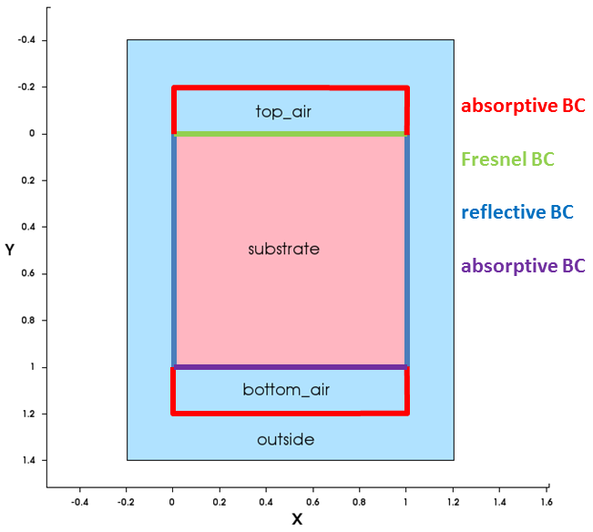
Figure 6. Boundary conditions for the raytracer. (Click image for full-size view.)
To control the BC for a particular interface, a region or material interface Physics section is used:
Physics (RegionInterface="region1/region2") {RaytraceBC(...)}
Physics (MaterialInterface="material1/material2") {RaytraceBC(...)}
The order of the regions to name the interface is not important, that is, region1/region2 and region2/region1 are equivalent.
By default, an interface behaves according to Snell's law and Fresnel equations. This case is called the Fresnel BC. However, other BCs are of interest as well. Commonly used BCs are:
- RaytraceBC(Fresnel), Fresnel BC, rays are propagated according to Snell's law and Fresnel equations; default BC.
- RaytraceBC(Reflectivity=1), reflective BC, rays are reflected to 100% according to Snell's law.
- RaytraceBC(Reflectivity=0 Transmittivity=0), absorptive BC, rays are stopped and absorbed to 100%.
- RaytraceBC(TMM(...)), TMM BC, the direction of rays is calculated according to Snell's law. However, reflection and transmission coefficients are computed using the TMM solver. This BC is used for very thin coatings, where interference effects cannot be neglected.
This results in the following BC settings for the example:
* absorptive BC at the side walls of Si
Physics(RegionInterface="substrate/outside") {
  RayTraceBC (Reflectivity=1)
}
* absorptive BC at the bottom of Si
Physics(RegionInterface="substrate/bottom_air") {
  RayTraceBC (Reflectivity=0 Transmittivity=0)
}
* absorptive BC for the rest
Physics(MaterialInterface="Gas/Gas") {
  RayTraceBC (Reflectivity=0 Transmittivity=0)
}
Click to view the command file sdevice_des.cmd.
5.4.2 Common Optical Solver Settings
The general setup is very similar to the example in Section 5.2 Calculating the Wavelength-Dependent Reflection Using TMM. However, some specific settings are explained here.
In contrast to the previous example, you want to change the incident angle of the light θ using the keyword Theta in the Excitation section, which in two dimensions defines the angle between the incident light direction and the +y-axis with counterclockwise orientation (see Figure 7).
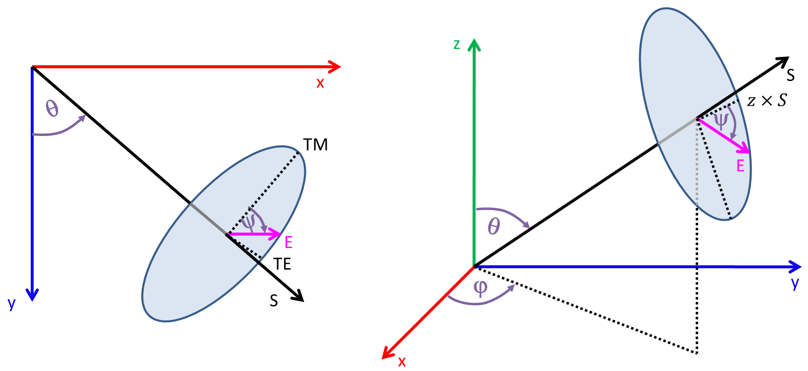
Figure 7. Angle definition for excitation direction and polarization in (left) two dimensions and (right) three dimensions. (Click image for full-size view.)
The excitation angle is defined with respect to the GCS and not with respect to the illumination window.
The polarization of the excitation is characterized by the polarization angle Ψ and can be set with the PolarizationAngle keyword:
- Ψ = 0 corresponds to p-polarization or TM.
- Ψ = 90 corresponds to s-polarization or TE.
Optionally, instead of PolarizationAngle, the Polarization keyword can be used, with Polarization = sin2(PolarizationAngle).
For convenience, in two dimensions, pure TE and TM polarization can be specified with Polarization=TE or Polarization=TM.
In three dimensions, an additional angle Phi is used to define the excitation direction, and the polarization can be specified using PolarizationAngle only.
This example uses the DF–ISE coordinate system in two dimensions, where the +y-axis points downwards. Therefore, Theta=0 is perpendicular to the device top surface, and Theta=90 is parallel.
Similar to the wavelength sweep in the previous example, you now want to perform an angular sweep, which is achieved by:
- Setting the starting angle Theta in the Excitation section:
Excitation ( Theta = 0 ... } - Performing an angular sweep in the Solve section:
Quasistationary ( DoZero InitialStep=@<1./179>@ MaxStep=@<1./179>@ Minstep=@<1./179>@ Goal {ModelParameter="Theta" value= 89.5 } ) { Optics } - Plotting the angle Theta into the .plt file:
CurrentPlot{
  ModelParameter="Theta"
}
5.4.3 Raytracer-Specific Settings
Some important commands control the raytracer are specified in the OpticalSolver(Raytracing(...)) section.
First, the starting rays must be distributed inside the illumination window. Several algorithms do this such as AutoPopulate, Equidistant, and MonteCarlo (refer to the Sentaurus™ Device User Guide for details). However, the easiest to start with is AutoPopulate, where only the number of rays must be specified:
        RayDistribution(
          Mode=AutoPopulate
          NumberOfRays = 1
        )
As the structure is planar and only reflection is of interest, one ray is sufficient.
Second, break criteria must be defined to control when tracing of a ray will be terminated. For this purpose, the raytracer provides two criteria:
        MinIntensity = 1e-4
        DepthLimit = 10000
MinIntensity stops the tracing of a ray if the ray intensity reaches the specified relative limit. In the above example, rays stop if their intensity becomes less than 1e-4 times their original intensity. DepthLimit stops the ray if it passes through more than the given number of interfaces.
MinIntensity is a more physical criterion that ensures correct results, while DepthLimit is more like an emergency break to avoid infinite loops for rays that are trapped in the structure and are never absorbed.
5.4.4 Calculating the Reflection
To extract optical quantities such as reflection or transmission, the raytracer can integrate photon fluxes across interfaces. To use this feature for a particular interface, the keyword PlotInterfaceFlux must be present in the RayTracing section. In addition, a BC must be defined for that interface. After this, for each region interface and impinging direction, Sentaurus Device plots the reflected, transmitted, and absorbed flux into the .plt file (see Figure 8).
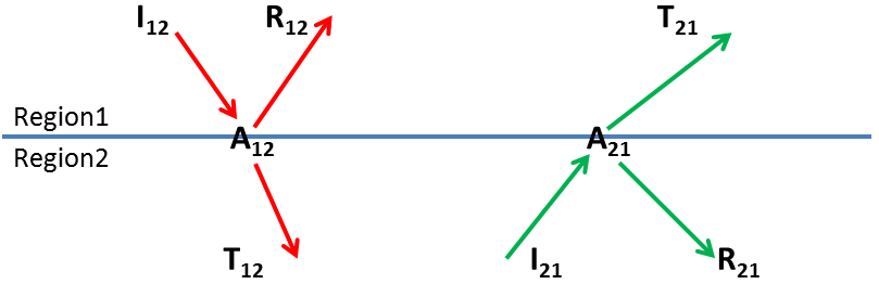
Figure 8. Calculating the reflection using the raytracer. (Click the image for full-size view.)
Therefore, at each interface, you can calculate the incident photon flux using the formula:
\[ R= {R_{12} + T_{21}} / {I_{12}} = {R_{12} + T_{21}} / {R_{12} + T_{12} + A_{12}} \]
For this example, the reflection, which is the number of reflected photons Nr divided by the number of impinging photons Nin, will be calculated in Sentaurus Visual.
Nr can be extracted using two different methods:
- As the absorbed photon flux of the top_air/outside interface.
- As the reflected photon flux of the top_air/substrate interface plus the transmitted photon flux of the substrate/top_air interface.
For Nin, you can do one of the following:
- Use the input photon flux that is written automatically to the .plt file.
- Calculate the incident photon flux at the top_air/substrate interface as the sum of the reflected, transmitted, and absorbed photon fluxes at that interface.
The calculation using method 1 for Nin and Nr in Sentaurus Visual looks like:
#- calculate reflection from input photons and absorbed photons
#- at top_air/outside interface
create_curve -name Nin1 -dataset $ds($n) -axisX $varTheta \
  -axisY "RaytracePhoton Input" ;# 1/s
create_curve -name Nr1  -dataset $ds($n) -axisX $varTheta \
  -axisY "RaytraceInterfaceFlux A(top_air/outside)" ;# 1/s
create_curve -name R1($n)  -function "<Nr1>/<Nin1>"
Using method 2 in Sentaurus Visual looks like:
#- calculate reflection from top_air/substrate interface only
create_curve -name R12 -dataset $ds($n) -axisX $varTheta \
  -axisY "RaytraceInterfaceFlux R(top_air/substrate)" ;# 1/s
create_curve -name T12 -dataset $ds($n) -axisX $varTheta \
  -axisY "RaytraceInterfaceFlux T(top_air/substrate)" ;# 1/s
create_curve -name A12 -dataset $ds($n) -axisX $varTheta \
  -axisY "RaytraceInterfaceFlux A(top_air/substrate)" ;# 1/s
create_curve -name T21 -dataset $ds($n) -axisX $varTheta \
  -axisY "RaytraceInterfaceFlux T(substrate/top_air)" ;# 1/s
  create_curve -name I12  -function "<R12>+<T12>+<A12>"
create_curve -name R2($n)  -function "(<R12>+<T21>)/<I12>"
The first region name in the interface name (for example, R(top_air/substrate)) denotes the region from where the ray originated before reaching the interface.
Click to view the complete command file svisual_vis.tcl.
Finally, clicking the Run Selected Visualizer Nodes Together toolbar button generates the required reflection versus incident angle plot (compare Section 2.7 Visualizing Selected Nodes Together). The reflection calculated according to the first and second methods as previously described are identical as expected (see Figure 9).
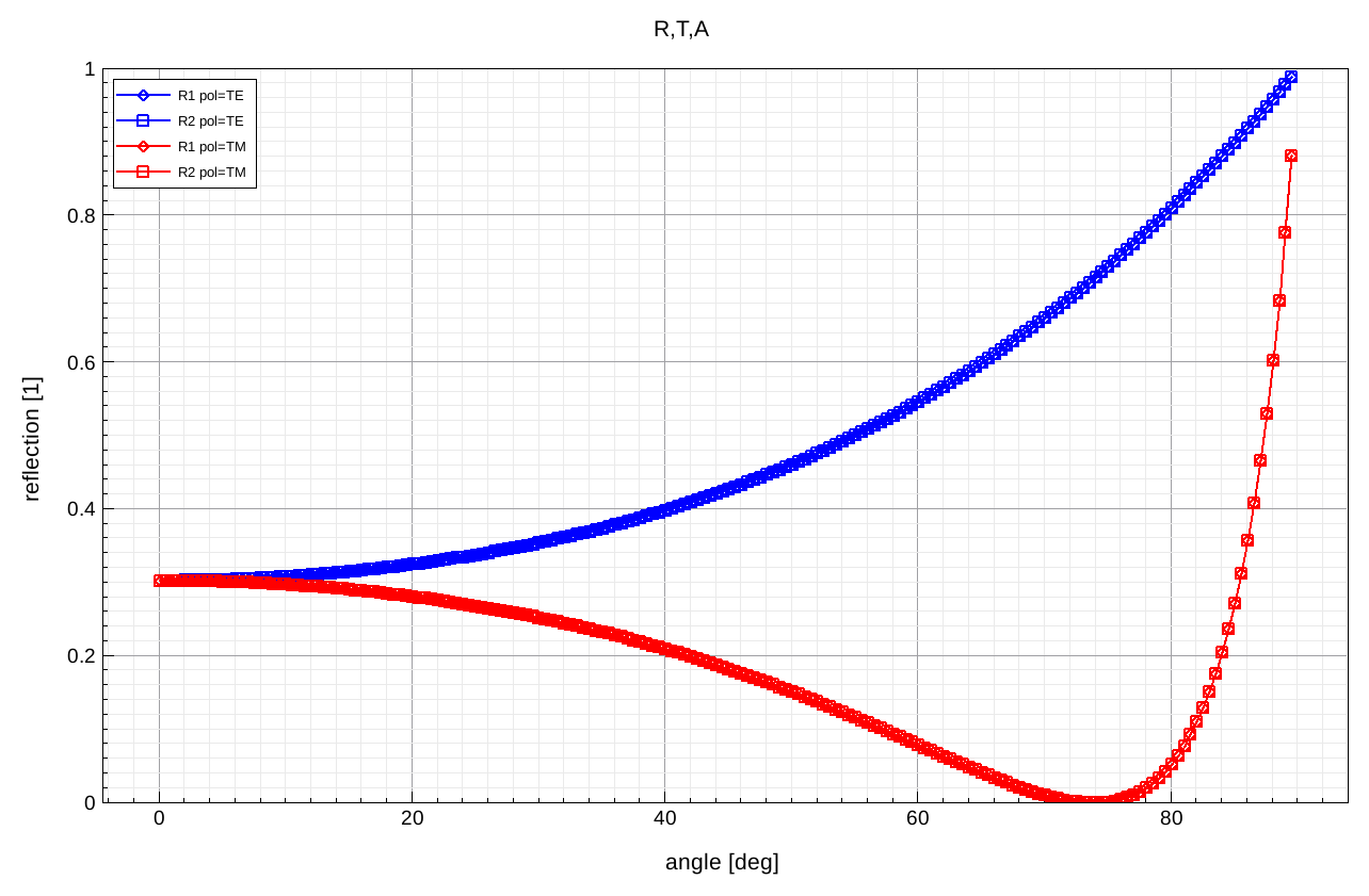
Figure 9. Reflection versus incident angle for TE and TM polarization using the raytracer. (Click image for full-size view.)
5.5 Calculating the White Light Photocurrent of a 3D Photodiode Using Raytracing
This section discusses combined optical and electrical equations, and addresses spectral illumination. As an example, the illuminated short-circuit current of a 3D photodiode is calculated using the raytracer. To optimize light coupling, the light-exposed silicon will be covered by a single nitride layer, which serves as an antireflective coating.
The complete project can be investigated from within Sentaurus Workbench in the directory Applications_Library/GettingStarted/sdevice/opto/rt-jsc-3d.
Similarly as in Section 5.4 Calculating the Angular-Dependent Reflection Using Raytracing, a top_air region and a bottom_air region are added to the structure, and the entire device is surrounded by an air region. This is done to give access to the boundary conditions of the top, bottom, and sidewalls (see Figure 10) by specifying interface Physics sections in the Sentaurus Device command file.
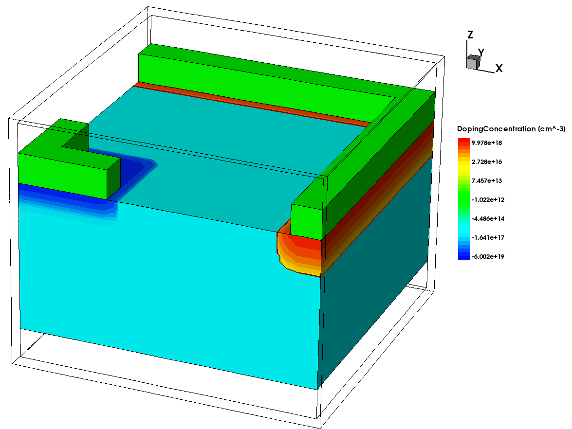
Figure 10. Boundary and doping of the 3D photodiode. Note the black wireframe that marks the surrounding region needed to define boundary conditions. (Click the image for full-size view.)
5.5.1 TMM Boundary Condition
To improve light coupling, antireflective coatings are widely used. These layers are typically in the range of wavelength, therefore, interference effects are crucial. On the other hand, they are typically electrically inactive, so they do not contribute to the optical generation and can be neglected in the electrical simulation.
A common approach to model such thin coatings with the raytracer is to collapse the coating layers onto the interface, and then to calculate the reflection and transmission coefficients using the TMM solver.
In the example, at the top_air substrate interface, a 75 nm thick nitride is defined with the lines:
Physics (RegionInterface="top_air/substrate") {
  RayTraceBC(
    TMM(
      ReferenceRegion = "top_air"
      LayerStructure {
        75e-3 "Nitride"
      }
    )
  )
}
Click to view the complete command file sdevice_des.cmd.
5.5.2 Illumination in Three Dimensions
As the device coordinate system is the unified coordinate system (UCS), the top of the device is in the –x-direction. To illuminate the device from the top, the excitation direction must be in the +x-direction. This can be achieved by setting Theta=90 and Phi=0 in the Excitation section (see Figure 7), or by simply specifying fromTop, which does this automatically for you:
    Excitation (
      fromTop
      PolarizationAngle = 45.
      Window (
        Origin = (-1.2, 2.5, 2.5)
        Rectangle(dx=5 dy=5)
      )
    )
Figure 11 illustrates the alignment of the illumination window with the device. The illumination window must cover the entire device – without the "outside" region – slightly above the top of the metal contacts.
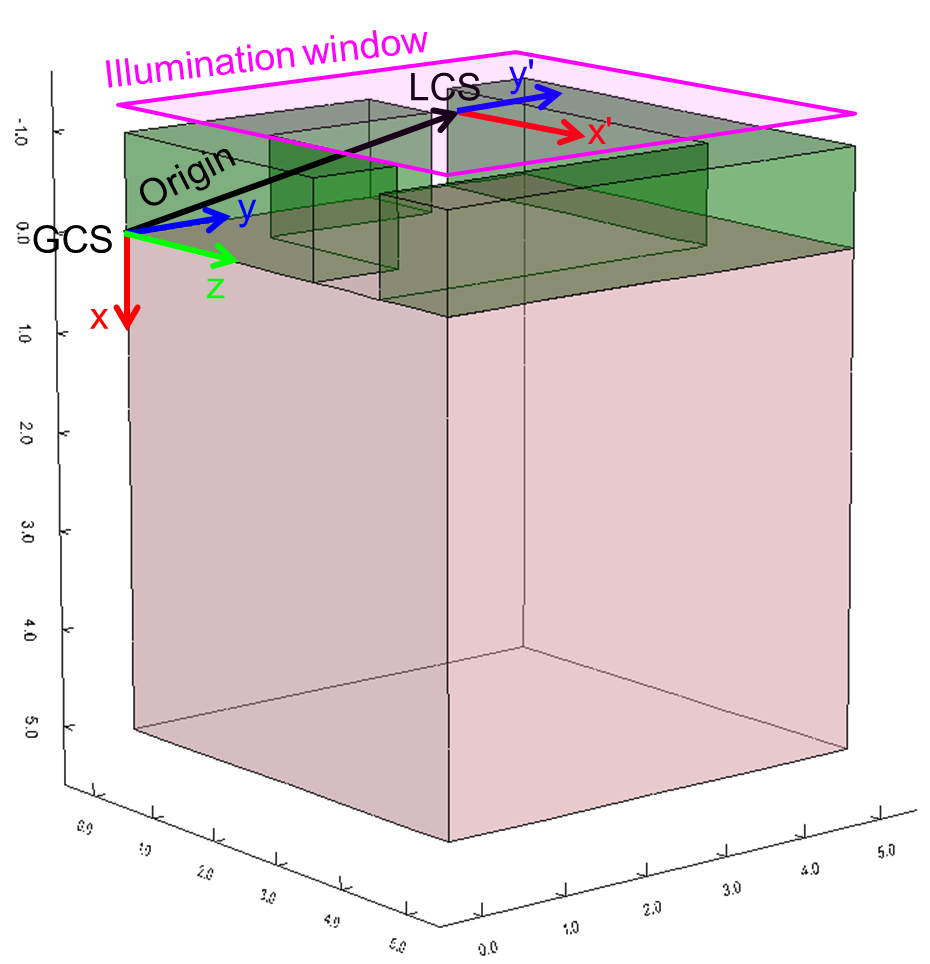
Figure 11. Alignment of the illumination window with the device. (Click image for full-size view.)
To accomplish this, you must shift the origin of the LCS (compare to Section 5.2 Calculating the Wavelength-Dependent Reflection Using TMM) horizontally to the center of the device (2.5, 2.5), where the total width of the device is 5 μm and 1.2 μm above the silicon surface.
Next, the LCS (x', y') must be rotated such that x' points in the z-direction and y' points in the y-direction of the GCS (see Figure 11). Manually, you would achieve this with the following keywords:
Window (...
  xDirection=(0,0,1)
  yDirection=(0,1,0)
  ...
)
However, in this example, fromTop does it automatically for you.
The width of the illumination rectangle in the x-direction and the y-direction is specified with the keywords dx and dy. If relative parameters such as dx are chosen to define the geometry extent, instead of absolute parameters such as corner1 (or x1 in two dimensions), the illumination window geometry is positioned such that the center of the geometry is at the origin of the LCS. As the origin of LCS is at (2.5, 2.5) and the rectangle extends 5 μm in each direction, the entire area from (0, 0) to (5, 5) is covered by the illumination window.
Distribution of the rays, in this case, is performed in Equidistant mode, specifying the distance between the starting rays in the x-direction and y-direction:
        RayDistribution(
          Mode=Equidistant
          Dx=0.5
          Dy=0.5
        )
In the case of 3D simulations, the number of rays might increase rapidly and, with this, also the elements in the raytree increase exponentially. Therefore, the computer memory limits the simulation. To work around memory limitation, you can specify the option CompactMemoryOption in the Raytracing(...) section, which reduces the memory need dramatically, due to sequential computation. However, plotting of the raytree is not available with this option.
Another way to optimize runtime and memory usage is to use a different tracing algorithm. By default, a deterministic algorithm is used. This means that, whenever a ray hits an interface, the ray is split into a reflected ray and a transmitted ray, and both of them are followed until they leave the device or a break criterion is met.
To change from an exponential behavior to a more efficient linear behavior, the raytracer offers the MonteCarlo algorithm. In this case, whenever a ray hits an interface, either the reflected ray or the transmitted ray is followed, depending on a random number, weighted with the reflection and transmission coefficients. Therefore, if an interface has 30% reflectance, three rays out of 10 rays are reflected, and seven are transmitted.
5.5.3 Extracting Results
The simulation is run by solving electrical equations only. Nevertheless, optics are solved because when Sentaurus Device is instructed to solve the transport equations for electron and holes, it detects that the optical generation term is not updated and will call the optical solver to update it. Therefore, no explicit call of the Optics section is necessary in this case.
Depending on the device structure and optical injection level, convergence might be problematic if the device is overwhelmed with optically generated carriers from the beginning. It is advisable to first solve transport in the dark, and only then switch on the light. This can be achieved by setting scaling=0 in the OpticalGeneration section:
    OpticalGeneration (
      Scaling=0
    ...)
In the Solve section, you first solve transport in the dark:
Solve{
  NewCurrentPrefix="tmp_"
  Poisson
  Coupled (Iterations=100) { poisson electron hole  }
Note that you have redirected the current file to tmp_n@node@_des.plt as these temporary preiterations are not required in the final results.
Then, you switch on the light by ramping the scaling parameter to the required value. Ensure that extrapolation is switched off to improve convergence by specifying -Extrapolate either globally in the Math section or, at least, in the Quasistationary statement:
  Quasistationary (
    InitialStep= 1e-1 MaxStep= 0.5
    -Extrapolate * better convergence when switching on light
    Goal { ModelParameter= "Scaling" Value= 100 }
  ){
    Coupled(Iterations=12) {Poisson Electron Hole}
  }
In the end, you switch back the current file to n@node@_des.plt and recalculate the required illuminated short-circuit current:
  NewCurrentPrefix=""
  Coupled { poisson electron hole }
As a result, the photogenerated current jph is extracted by integrating the optical generation inside the semiconductor region, and the short-circuit current jsc at the contact with a Sentaurus Visual node. The results are returned to Sentaurus Workbench (see Figure 12).
Click to view the complete command file svisual_vis.tcl.
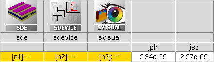
Figure 12. Snapshot of Sentaurus Workbench project.
5.6 Calculating Quantum Efficiency Versus Frequency Using Optical AC Analysis
This section demonstrates how to set up optical AC analysis based on the small-signal AC analysis method in Section 3.4 Small-Signal AC Analysis. As an example, the transfer matrix method (TMM) solver is used to illuminate a 2D photodiode at different wavelengths in the visual spectrum. Quantum efficiency versus frequency is computed and the 3 dB point is extracted from the curves for each wavelength.
The complete project can be investigated from within Sentaurus Workbench in the directory Applications_Library/GettingStarted/sdevice/opto/OpticalAC.
During optical AC analysis, a small perturbation is applied to the optical generation rate. The resulting small-signal device current perturbations on each electrode are then used to compute the real and imaginary parts of the quantum efficiency. Sentaurus Device saves the real and imaginary parts of the quantum efficiency in the AC output file as photo_a (real part) and photo_c (imaginary part) for each electrode.
For a detailed description of the real and imaginary parts of the quantum efficiency equation, see the Sentaurus™ Device User Guide.
Click to view the primary file sdevice_des.cmd.
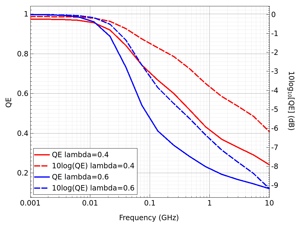
Figure 13. Quantum efficiency versus frequency (solid lines) and 10log[QE] versus frequency (dashed lines). (Click image for full-size view.)
The 3 dB point is determined by plotting the 10log[QE] curve and then extracting the value of frequency at –3 dB (see Figure 13). In this example, the extracted 3 dB points for the 400 nm and 600 nm curves are 0.516 GHz and 0.087 GHz, respectively. The results are returned to Sentaurus Workbench (see Figure 14).
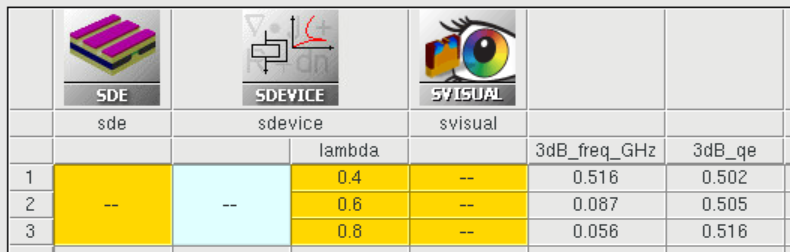
Figure 14. Snapshot of Sentaurus Workbench project. (Click image for full-size view.)
To use optical AC analysis, first set up a mixed-mode simulation as described in Section 3.2 Mixed-Mode Simulations. To activate optical AC analysis, add the keyword Optical in the ACCoupled statement.
If an element is excluded (Exclude statement) in optical AC (this is usually the case for voltage sources in regular AC simulation), then this means that this element is not present in the simulated circuit and, correspondingly, it provides zero AC current for all branches connected to the element. Therefore, do not exclude voltage sources in optical AC analysis.
Copyright © 2022 Synopsys, Inc. All rights reserved.