
Sentaurus Interconnect
2. Example: 3D Damascene Structure
2.1 Overview
2.2 Defining Initial 3D Grid
2.3 Defining Initial Simulation Domain
2.4 Initializing the Simulation
2.5 Setting Up a Meshing Strategy
2.6 Defining Mesh Refinement
2.7 Performing Etching and Deposition
2.8 Solving Stresses
2.9 Extracting 1D Profiles
2.10 Defining Contacts
2.11 Defining Physical Loads
2.12 Thermal and Electrical Analyses Simulation
Objectives
- To demonstrate how to simulate a damascene structure in three dimensions.
2.1 Overview
In this section, a typical simulation flow is demonstrated with a damascene structure in three dimensions. The structure is composed of two metals and a via (all copper). Many widely used process and control commands are introduced to perform the following types of simulation:
- Stress
- Structure generation and process
- Coupled thermal and electrical analyses
Other relevant topics are covered such as controlling meshing, defining contacts and supplies, and saving snapshots.
2.2 Defining Initial 3D Grid
The initial 3D grid is defined with line commands:
line x location= 0.0      spacing= 0.05<um> tag= subTop
line x location= 0.1<um>  spacing= 0.05<um> tag= subBottom
line y location=-0.1<um>  spacing= 0.05<um>
line y location= 0.05<um> spacing= 0.05<um>
line z location= 0.0<um>  spacing= 0.1<um>
line z location= 0.7<um>  spacing= 0.1<um>
The first argument of the line command specifies the direction of the grid. The grid spacing is defined by pairs of the location and spacing arguments. The argument spacing defines the spacing between two grid lines at the specified location. Sentaurus Interconnect expands or compresses the grid spacing linearly between the two locations defined in the line command.
Sentaurus Interconnect uses coordinate systems such that 1D, 2D, and 3D simulations are consistent. Most importantly, the positive x-axis always points into the wafer. In two and three dimensions, the positive y-axis points to the right and, in three dimensions, the positive z-axis points out of the page.
Units in Sentaurus Interconnect can be specified explicitly by giving the
units in angle brackets. For most cases, the default unit of length is micrometer. Therefore,
location=2.0<um> and location=2.0 are equivalent. In this section,
units are given explicitly.
The unified coordinate system (UCS) is switched on by default (math coord.ucs),
so the axes in Sentaurus Visual match the axes in the command file of Sentaurus Interconnect.
You can label a line with the tag keyword for later use in the region command.
2.3 Defining Initial Simulation Domain
To define the initial simulation domain, use the region command. Many, if not most, simulations start with a block of silicon. The shorthand for this situation is to define a region of silicon that spans all defined lines:
region Silicon
You also can use the region command to define a new region between specified lines. To limit the size of the region to be less than all defined lines, the lines must be given a label with the tag argument, which is defined in the line command. These labels are used in the region command with the xlo, xhi, ylo, yhi, zlo, and zhi arguments.
2.4 Initializing the Simulation
To initialize the simulation, use the init command:
init wafer.orient= { 0 0 1 } notch.direction= { 1 1 0 }
Here, the wafer orientation is set to {0 0 1}, and the flat orientation is set to {1 1 0}; these are the defaults.
The init command can be used to initialize the initial impurity and many other definitions, and to load previous simulations.
2.5 Setting Up a Meshing Strategy
The initial grid is valid until the first command that changes the geometry, such as deposition or etching. For these steps, a remeshing strategy must be defined.
The meshing engine Sentaurus Mesh tries to preserve the initial mesh as much as possible and only modifies the mesh in the new layers and in the vicinity of the new interfaces.
To define a remeshing strategy, use:
pdbSet Grid SnMesh min.normal.size  0.020 ;# 20nm
pdbSet Grid SnMesh max.lateral.size 0.100 ;# 100nm
pdbSet Grid SnMesh normal.growth.ratio.3d 2.0
where:
- min.normal.size determines the grid spacing of the first layer starting from the interface.
- max.lateral.size limits not only the lateral grid spacing, but also the maximum grid spacing anywhere.
- normal.growth.ratio.3d determines how fast the grid spacing can increase from one layer to another.
2.6 Defining Mesh Refinement
Usually, localized refinement is defined by introducing refinement boxes. This strategy prevents excessive meshing that can result if mesh refinement is based solely on the line command (with the spacing argument). Lines specified with the line command run the entire length (or breadth or depth) of the structure.
The refinement boxes can be inserted at any time during the simulation. The simplest form of a refinement box used in this example consists of minimum and maximum coordinates where the refinement box is valid, and the local maximum mesh spacing is in the x-, y-, and z-direction. A refinement box specified for a 2D simulation will be applied to a 1D simulation if it is valid for y=0.0. Similarly, a 3D refinement box will be applied if it covers z=0.0.
The following refinement boxes specify refinement criteria defined by coordinates or materials:
refinebox name= active min= { -0.65 -0.1 0.0 } max= { -0.1 0.05 0.7 } \
	xrefine= 100<nm> yrefine= 100<nm> zrefine= 100<nm>
refinebox name= metal materials= Copper \
	xrefine= 50<nm> yrefine= 50<nm> zrefine= 50<nm>
The other type of refinement box used in this example is an interface refinement. This type of interface is a graded refinement that is refined near an interface in the perpendicular direction and relaxed away from the interface. Using the refinebox command, you can specify interface refinement using either the interface.materials argument or the interface.mat.pairs argument:
refinebox interface.materials= { Copper Nitride Oxide }
- Use interface.materials to indicate that refinement will occur at all interfaces to the specified materials.
- Use interface.mat.pairs to choose interface refinement only at the interface of two specific materials, Multiple interface material pairs can be specified, for example: interface.mat.pairs= {Copper Oxide Copper Silicon}
The refinebox command only specifies a refinement criterion, but the mesh is not changed. The grid remesh command forces a remesh.
2.7 Performing Etching and Deposition
The structure is created with etching and deposition operations to simulate processing steps. Masks can be used in these operations, and they must be defined before use:
mask clear
mask name= metal_1 left= 0.0 right= 0.1 front= 0.0 back= 0.45
mask name= via_12 left= 0.025 right= 0.1 front= 0.3 back= 0.4
mask name= metal_2 left= 0.0 right= 0.1 front= 0.25 back= 0.7
Masks can be inverted using the negative option:
mask name= test left= -1.0 right= 1.0 front= -1.0 back= 1.0 negative
The damascene structure is defined with a series of etching and deposition steps:
deposit Oxide temperature= 250<C> thickness= 0.1 type= isotropic
deposit Oxide temperature= 250<C> thickness= 0.2 type= isotropic
deposit Photoresist thickness= 0.1 type= isotropic mask= metal_1
etch Oxide temperature= 25<C> thickness= 0.2 type= anisotropic
deposit Copper temperature= 250<C> coord= -0.3 type= fill
strip Photoresist
deposit Nitride temperature= 250<C> coord= -0.35 type= fill
deposit Oxide temperature= 250<C> thickness= 0.1 type= isotropic
deposit Photoresist thickness= 0.1 type= isotropic mask= via_12
etch Oxide temperature= 25<C> thickness= 0.11 type= anisotropic
etch Nitride temperature= 25<C> thickness= 0.1 type= anisotropic
deposit Copper temperature= 250<C> coord= -0.46 type= fill
strip Photoresist
deposit Oxide temperature= 250<C> coord= -0.65 type= fill
deposit Photoresist thickness= 0.1 type= isotropic mask= metal_2
etch Oxide temperature= 0<C> thickness= 0.2 type= anisotropic
deposit Copper temperature= 250<C> coord= -0.65 type= fill
strip Photoresist
deposit Nitride temperature= 250<C> coord= -0.7 type= fill
Intrinsic stresses can be added to a deposited material using the stressdata command after deposition:
stressdata Oxide sxxi= 1e3<MPa> syyi= 1e3<MPa> szzi= 1e3<MPa>
A stress relaxation step is called after each etch or deposit command. You can switch off this behavior with the PDB parameter:
pdbSet Mechanics EtchDepoRelax 0
Furthermore, you can switch on the following PDB parameter to trace all temperature ramps in fabrication steps and to solve thermal mismatch strains and stresses:
pdbSet Mechanics StressHistory 1
By default, the simulation dimension is promoted only when necessary. Therefore, until a mask is introduced, the simulation remains 1D. Similarly, when going from two dimensions to three dimensions, until a 3D mask is introduced (one that varies in the z-direction in the defined simulation domain), the simulation remains 2D.
Figure 1 shows the final structure where the substrate and Gas regions are hidden. For a better view, the other regions are transparent, except Copper and Nitride.
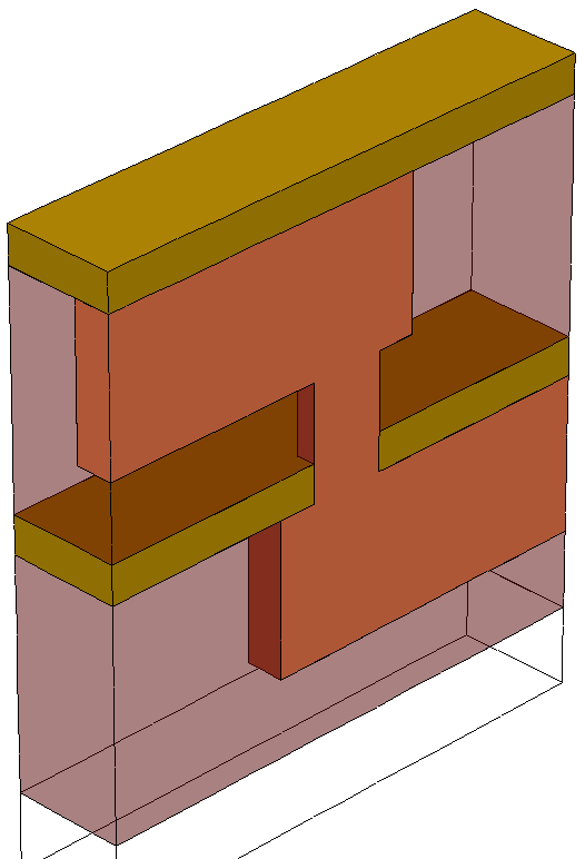
Figure 1. Final damascene structure. (Click image for full-size view.)
2.8 Solving Stresses
Before solving stresses, the mode command is used to identify all effects that will be solved. In this step, only the mechanics option is used. The solve command then is called to solve stresses at certain temperatures (or temperature ramps). For example:
mode mechanics

solve temperature= 25
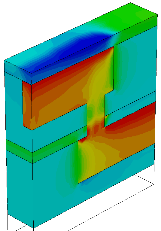
Figure 2. Stress distribution from thermal mismatch, along the z-direction. (Click image for full-size view.)
2.9 Extracting 1D Profiles
You can save 1D profiles at any point in the process flow, for example:
SetPlxList { StressEL_xx StressEL_yy StressEL_zz }

WritePlx damascene_via.plx y= 0.04 z= 0.35 Copper
or:
struct tdr= n@node@_via.tdr y= 0.04 z= 0.35
2.10 Defining Contacts
Besides stress simulation, the thermal and electrical analyses simulation is performed for the structure. To do that, contacts are defined and then are supplied with certain electrical, electrostatic, or thermal boundary conditions, such as voltage, and temperature.
Contacts are added to the structure using the contact command. There are two types of contact specification:
- For a box contact, you specify a box and a material, and all interfaces of that material that are inside the box become the contact.
- For a point contact, you specify a point inside a chosen region. The chosen region is removed, and all interfaces between the chosen region and bulk materials become part of the contact.
In the following example, only box-type contacts are defined:
contact Copper name= upper box sidewall \
	xlo= -0.65 xhi= -0.45 ylo= 0.0 yhi= 0.05 zlo= 0.7 zhi= 0.7
contact Copper name= lower box sidewall \
	xlo= -0.30 xhi= -0.10 ylo= 0.0 yhi= 0.05 zlo= 0.0 zhi= 0.0
contact Silicon name= tm0 box  \
	xlo= 0.0 xhi= 0.0 ylo= -0.1 yhi= 0.05 zlo= 0.0 zhi= 0.7
contact Nitride name= tm1 box  \
	xlo= -0.7 xhi= -0.7 ylo= -0.1 yhi= 0.05 zlo= 0.0 zhi= 0.7
2.11 Defining Physical Loads
The supply command is used to supply physical loads to contacts, regions, or boundaries, depending on the types of loading. You can define the following physical loadings:
- Electrical such as current and voltage
- Thermal such as temperature and power
- Mechanical such as displacement and force
The following commands define electrical and thermal supplies on the contacts:
supply contact.name= upper voltage= 0.1<V>
supply contact.name= lower voltage= 0.0<V>
supply contact.name= tm0 temperature= 100<C>
supply contact.name= tm1 temperature= 25<C>
2.12 Thermal and Electrical Analyses Simulation
To perform thermal and electrical analyses simulation, append the mode command to include all effects intended to be coupled together before the solve command:
mode mechanics current thermal
solve time= 1<s>
After solving, the voltage and temperature distributions are shown in Figure 3 and Figure 4 for the damascene structure, respectively.
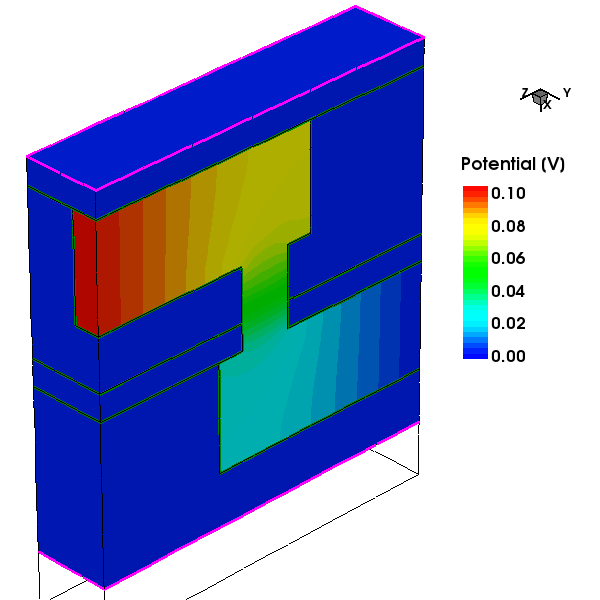
Figure 3. Potential distribution: potential is set to 0.1 V for upper copper sidewall and 0.0 V for lower one. (Click image for full-size view.)
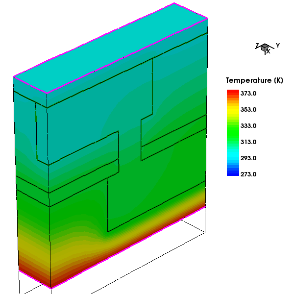
Figure 4. Temperature distribution: temperature is set to 373 K (100°C) on the bottom and 298 K (25°C) on the top. (Click image for full-size view.)
Copyright © 2022 Synopsys, Inc. All rights reserved.