 main menu
| module menu
| << previous section
| next section >>
main menu
| module menu
| << previous section
| next section >>
Sentaurus Interconnect
6. Example: Inverter
6.1 Overview
6.2 Defining New Materials
6.3 Defining the Initial 3D Grid
6.4 Defining the Initial Simulation Domain
6.5 Initializing the Simulation
6.6 Setting Up Meshing and Refinement Strategies
6.7 Performing Etching and Deposition
6.8 Defining the Contacts and Supplies
6.9 Electrostatic Simulation
Objectives
- To demonstrate how to build a simplified inverter and to run the electrostatic analysis with it.
6.1 Overview
The section shows the steps to build a simplified inverter and to run the electrostatic analysis with it. Besides the commands that have been used in the damascene example, a few more commands will be introduced.
6.2 Defining New Materials
You can create new materials from existing ones. All material properties are inherited from the source material. The following command creates a new material DIEL from Oxide:
mater add name= DIEL new.like= Oxide
After the definition, the material properties are changed with pdbSet commands. The dielectric constant is changed to 3.0:
pdbSet DIEL Potential Permittivity 3.0
6.3 Defining the Initial 3D Grid
The initial 3D grid is defined with line commands:
line x location= 0.0
line x location= 0.1
line y location= 0.0
line y location= 1.5
line z location= 0.0
line z location= 1.0
The default unit is micrometer.
6.4 Defining the Initial Simulation Domain
The initial simulation domain is defined with the region command, and the material is silicon, which serves as the ground in this inverter structure:
region Silicon
6.5 Initializing the Simulation
The simulation is initialized with default settings:
init
6.6 Setting Up Meshing and Refinement Strategies
Next, global meshing and local refinement strategies are defined. For refinements, only interface refinement is used in the example:
pdbSet Grid SnMesh min.normal.size 0.050
refinebox min.normal.size= 0.05 interface.materials= { Copper DIEL }
6.7 Performing Etching and Deposition
First, masks must be defined for etching operations. While a simple mask can be defined by specifying its boundary, a more complicated mask can be defined from one or more polygons like masks m1 and m3 here:
polygon name= p1 \
  segments= {0.55 0.50 1.6 0.50 1.6 0.65 1.4 0.65 1.4 0.55 0.55 0.55}
polygon name= p2 min= {0.4 0.3}   max= {0.7 0.7}  rectangle
polygon name= p3 min= {1.25 0.35} max= {1.75 0.5} rectangle
polygon name= p4 min= {1.4 0.55}  max= {1.6 0.65} rectangle

mask clear
mask name= m1 polygons= {p1} negative
mask name= m2 left= 1.47 right= 1.53 front= 0.55 back= 0.60 negative
mask name= m3 polygons= {p2 p3 p4}
The stress simulation is omitted in this example, so the following two switches are turned off before any deposition or etching steps:
pdbSet Mechanics EtchDepoRelax 0
pdbSet Mechanics StressHistory 0
Second, the inverter structure is defined with a set of deposit and etch commands. Initially, only half of the structure is constructed:
deposit DIEL thickness= 0.1 isotropic
deposit Copper thickness= 0.03 anisotropic mask= m1

deposit DIEL coord= -0.35 fill
etch    DIEL thickness= 0.3 anisotropic mask= m2
deposit Copper coord= -0.35 fill

deposit Copper coord= -0.4 fill
etch    Copper thickness= 0.1 anisotropic mask= m3
deposit DIEL coord= -0.9 fill
Then, the transform command reflects the half-structure to the whole structure:
transform reflect right
Figure 1 shows the final structure. The DIEL region is not displayed for better visualization.
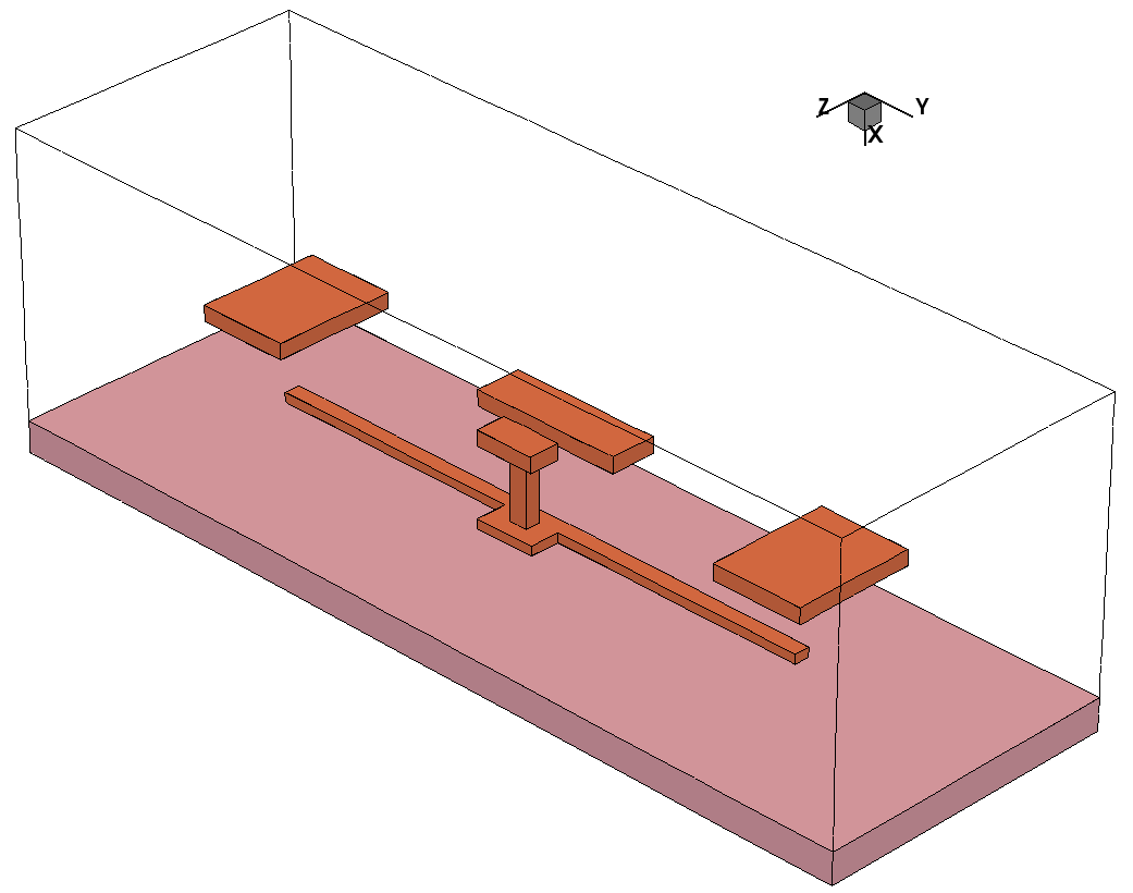
Figure 1. Final inverter structure. (Click image for full-size view.)
6.8 Defining the Contacts and Supplies
Point-type contacts are defined in this example for the etch metal region and then are supplied with a fixed voltage. One contact is set to 1 V and the others are set to 0 V:
contact name= c0 x=  0.05 y= 1.5 z= 0.5 point Silicon !replace
contact name= c1 x= -0.38 y= 1.5 z= 0.6 point Copper !replace
contact name= c2 x= -0.38 y= 1.5 z= 0.4 point Copper !replace
contact name= c3 x= -0.38 y= 0.6 z= 0.5 point Copper !replace
contact name= c4 x= -0.38 y= 2.4 z= 0.5 point Copper !replace

supply contact.name= c0 voltage= 0.0
supply contact.name= c1 voltage= 0.0
supply contact.name= c2 voltage= 1.0
supply contact.name= c3 voltage= 0.0
6.9 Electrostatic Simulation
To perform the electrostatic simulation, the mode command must be called before the solve command:
mode electrostatic

solve info= 2
Figure 2 shows a snapshot after the electrostatic simulation is completed. Only half of the structure is shown and the dielectric region is transparent.
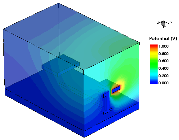
Figure 2. Snapshot saved after the electrostatic analysis is completed. (Click image for full-size view.)
main menu | module menu | << previous section | next section >>
Copyright © 2022 Synopsys, Inc. All rights reserved.