
Sentaurus Device
14. Special Focus: Stress- and Orientation-Dependent MOS Simulation
14.1 Overview
14.2 Specifying the Simulation Orientation
14.3 Reading Stress Profiles From a TDR File
14.4 IALMob Model and Auto-Orientation Feature
14.5 IALMob Model With High-k Mobility Models
14.6 Quantum Corrections on Carrier Density
14.7 Effects of Stress on Band Structure and Carrier Density
14.8 Effects of Stress on Band Structure and Mobility
Objectives
- To demonstrate stress-dependent and orientation-dependent MOS simulations in Sentaurus Device.
14.1 Overview
Quantum effects and stress-induced changes to the band structure must be considered to compute the correct dependency of the carrier concentration on the quasi-Fermi level. In addition, such effects influence the carrier mobility by changing the number of available final scattering states for intravalley and intervalley scattering mechanisms, and the effective conductivity masses. Moreover, interface-scattering mechanisms can depend on the channel interface orientation and the channel direction, requiring mobility models with varying parameterization, dependent on orientation.
Sentaurus Device provides various models to accomplish such dependencies. The project Applications_Library/GettingStarted/sdevice/MultiValleyMOS demonstrates the influence of device orientation and uniaxial stress along the x-direction on the Id–Vg characteristics for a 45 nm NMOS and PMOS. In particular, it demonstrates how to:
- Specify the device simulation orientation.
- Read stress profiles from a TDR file.
- Use the inversion and accumulation layer mobility (IALMob) model together with the auto-orientation feature.
- Combine density-gradient quantum corrections with stress-induced changes to the band structure.
- Model the influence of stress, device orientation, and quantum effects onto the channel mobility.
14.2 Specifying the Simulation Orientation
The orientation of the simulation coordinate system must be specified with respect to the crystallographic directions using the LatticeParameters section of the parameter file. For example, the following specifies the x-coordinate axis of the simulation domain to point in the [1 0 0] direction, while the y-axis is oriented along the [011] direction of the crystal:
LatticeParameters {
  X = (1,  0,  0)
  Y = (0, -1, -1)
}
Figure 1 shows the simulation coordinate axes with respect to the example MOS geometry.
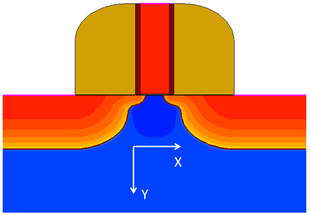
Figure 1. NMOS with simulation coordinate axes indicated. (Click image for full-size view.)
In this project, the Sentaurus Workbench variables @surface@ and @channel@ define the orientation specifications in the parameter file, for (channel interface orientation)/<channel direction> combinations (001)/<100>, (001)/<011>, (011)/<100>, and (011)/<011> in an NMOS and a PMOS.
Click to view the primary file sdevice.par.
14.3 Reading Stress Profiles From a TDR File
Realistic stress profiles are usually calculated within Sentaurus Process. However, in this project, a simple uniform uniaxial stress profile with the only nonzero component being σXX is specified within Sentaurus Structure Editor. In either case, the TDR file containing the stress data is specified by the Piezo file within the File section of the Sentaurus Device command file:
File {
  Grid      = "@tdr@"
  Piezo     = "@tdr@"
...}
By default, the meanings of the stress components read from the TDR file are assumed to refer to the same simulation coordinate system as specified in Sentaurus Device. Explicitly, this is expressed by the Math setting:
Math {
  CoordinateSystem { AsIs }
...}
For alternative specifications, see the Sentaurus™ Device User Guide, Chapter 2.
14.4 IALMob Model and Auto-Orientation Feature
These MOS simulations demonstrate the use of the inversion and accumulation layer mobility (IALMob) model. This model takes into account bulk phonon and impurity scattering as well as contributions due to surface roughness and surface phonon scatterings.
In Sentaurus Device, the IALMob model is selected as an option to the Enormal keyword of the Mobility specification, as shown here.
For the bulk part of the IALMob model, you select either the full Philips unified mobility model (PhuMob) or a reduced model. The full model is used by default. The reduced model, which neglects some terms related to minority carriers, is selected by setting the -FullPhuMob flag:
Physics (material= "Silicon") {
...
  Mobility(
    Enormal ( IALMob( AutoOrientation ) Lombardi_highk )
    HighFieldSaturation( EparallelToInterface )
  )
...}
Some additional parameter file specifications are required to use this model consistently with the literature:
- Sentaurus Device omits the calculation of the transverse field–dependent mobility model if the normal field is very small. Since the IALMob model calculates both doping-dependent and transverse field–dependent mobility, it must be called for all values of the normal field. This can be accomplished by setting EnormMinimum=0.0 in the IALMob section.
- To select the Hänsch model, specify the parameter α=1 in the
HighFieldDependence section. In addition, the exponent in the Hänsch
model is equal to 2, which can be specified by setting β0 = 2 and
βexp = 0, respectively:
IALMob {
        EnormMinimum    = 0.0           # [V/cm]
...}
HighFieldDependence {beta0 = 2.0 , 2.0 # [1] betaexp = 0.0 , 0.0 # [1] alpha = 1.0 , 1.0 # [1] ...}
Click to view the silicon parameter file Si.par.
It is well known that the surface-related scattering mechanism strongly depends on the channel interface orientation and the channel direction. To account for such a dependency on mobility surface orientation, named parameter sets for the IALMob model can be specified in the parameter file:
IALMob "name" { ... }
When the AutoOrientation option is activated, the model by default looks for and uses parameter sets named "100", "110", and "111" corresponding to surface orientations of {100}, {110}, and {111}:
IALMob "001" { ... }
IALMob "110" { ... }
IALMob "111" { ... }
The AutoOrientation option is activated inside the IALMob specification:
Physics (Material= "Silicon") { ...

  Mobility(
    ...
Enormal ( IALMob( AutoOrientation ) Lombardi_highk )
    ...
  )
}
14.5 IALMob Model With High-k Mobility Models
For devices with high-k materials in the gate stack, remote phonon and remote Coulomb scattering can contribute as mobility-limiting scattering mechanisms. Such contributions can be added by specifying the Lombardi_highk mobility model inside the Enormal mobility section:
Physics (Material= "Silicon") { ...

  Mobility(
    ...
Enormal ( IALMob( AutoOrientation ) Lombardi_highk )
    ...
  )
}
Besides the remote scattering terms, the Lombardi_highk model also contains surface roughness and surface phonon contributions. Such contributions are already taken into account by the IALMob model. Therefore, they are switched off in the Lombardi_highk model by appropriate parameter settings for alpha_lom_e and alpha_lom_h. Remote Coulomb scattering terms are assumed to be negligible in this example and are switched off as well. This is accomplished by setting the following Lombardi_highk parameters to zero:
Lombardi_highk {
 alpha_lom_e = 0.0
 alpha_lom_h = 0.0
 alpha_rcs_e = 0.0
 alpha_rcs_h = 0.0
}
14.6 Quantum Corrections on Carrier Density
Carrier quantization influences charge carrier density as well as carrier scattering and, consequently, carrier mobility. In this example, the density gradient model is used to account for the influence of quantization on carrier density, while the influence of quantum effects on mobility is taken into account by the modified local-density approximation (MLDA) model.
For quantum corrections on carrier density in NMOS and PMOS simulations, the density gradient model is activated for electrons or holes in the Physics section of the channel material (silicon) by the keyword eQuantumPotential (hQuantumPotential for holes):
Physics (Material = "Silicon") { ...
  eQuantumPotential
  eMultiValley(MLDA kpDOS -Density)
  ...
}
The density gradient model also supports the auto-orientation framework, which can be activated by specifying AutoOrientation as an argument to either eQuantumPotential or hQuantumPotential in the command file:
Physics (Material = "Silicon") { ...
  eQuantumPotential(AutoOrientation)
  eMultiValley(MLDA kpDOS -Density)
  ...
}
The flag -Density, used as an option to the MultiValley model, is required here to switch off additional quantum corrections on the density calculated by the quasi-1D MLDA model.
In addition to the changes in the Physics section, the equation for the density-gradient quantum corrections must be added to the set of coupled equations:
Solve {...
  { Coupled { Poisson Electron Hole eQuantumPotential} }
  ...
}
The MLDA model in this example is used only for effects on mobility.
14.7 Effects of Stress on Band Structure and Carrier Density
To take into account the strain-induced conduction and valence band-edge shifts as well as band-structure curvature changes, additional models must be activated. Besides the simpler models, the deformation potential model with the two-band k·p calculations for electrons and the six-band k·p model for holes are used in this example. These models are specified by the Piezo model settings in the Physics section as:
  Piezo(
    Model(
      DeformationPotential(ekp hkp minimum)
      DOS( emass hmass )
     ...
  )
)
The options ekp and hkp activate the k·p models for electrons and holes, respectively. The option minimum indicates to use the lowest (for the conduction band) or the topmost (for the valence band) band edge of the split bands as the new effective band edge.
The DOS(emass hmass) statement activates the calculation of a new effective density-of-states (DOS) for the strained lattice.
14.8 Effects of Stress on Band Structure and Mobility
Quantum corrections and stress effects on the band structure result in a modified effective conductivity mass tensor as well as modifications of the contributions due to different scattering mechanisms onto the mobility. To take such effects into account, hMultiValley with hSubband model specifications are required for holes:
Physics (Material= "Silicon") {
  hMultivalley(MLDA kpDOS -Density)
  ...
  Piezo (
    Model (
      ...
      Mobility( hSubband(Doping EffectiveMass Scattering(MLDA) )
        hSaturationFactor= 0.0
      )
    )
  )
}
The option MLDA in the hMultiValley statement activates the MLDA model to account for quantum effects on holes. The six-band k·p model for the strained band structure is activated by the option kpDOS. The flag -Density indicates that these models must be used only for the hSubband mobility model. Similarly, eMultiValley can be used for electrons.
The total hole-mobility tensor to be calculated can be written in the following general form, which can be applied to both bulk and inversion layer cases:
\[ μ↖{-}_{p} = q τ_0 ∑↙{i}{p_i} / {p} {τ_i}/{τ_0}(m↖{-}_{C,i})^{-1} \]
where:
- \({p_i}/{p}\) is a local hole-band occupancy.
- \( {τ_i}/{τ_0} \) is the ratio of stressed and unstressed relaxation times.
- \( (m↖{-}_{C,i})^{-1} \) is the inverse conductivity hole mass tensor.
The model accounts for the six-band hole-band structure in all terms of this equation. For the inversion regime, the model computes the six-band k·p MLDA DOS of each band. Finally, the model computes the mobility ratio (3x3 tensor), which corrects the relaxed current density.
Figure 2 shows the influence of the channel direction/surface orientation on the device Id–Vgs of the given PMOS.
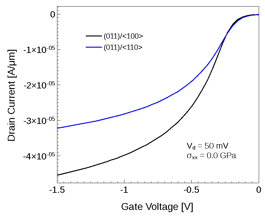
Figure 2. Id–Vgs for given (011) PMOS for <100> and <011> channel orientation. (Click image for full-size view.)
The option Doping of the subband model indicates that a carrier density and the corresponding Fermi-level according to the local doping will be used to compute the valley occupancies. Alternatively, the local carrier density can be used by specifying the Fermi keyword.
The option EffectiveMass of the subband model activates the calculation of the effective mass tensor.
The option Scattering(MLDA) of the subband model activates the scattering model, which defines the ratio of the stressed and unstressed valence-band momentum relaxation times τ/τ0. It considers acoustic phonon scattering, optical phonon emission, optical phonon absorption, and simplified impurity scattering. The option MLDA to the scattering model activates MLDA quantum corrections in the calculation of the valley relaxation times.
By default, the subband model uses unstrained mobility values according to the named parameter sets for the {100}, {110}, and {111} surface orientations. The parameter sets are assumed to be calibrated for the <110> channel direction. For other channel interface orientations, the set that fits best to one of these orientations is used.
For other combinations of surface and channel orientations, copy the project into your Sentaurus Workbench working directory and run it for configurations of interest.
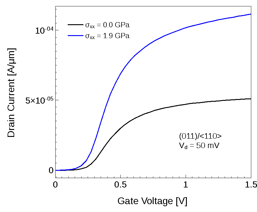
Figure 3. NMOS Id–Vgs at 0.05 V drain voltage for the given (100)/<011> channel orientations, with and without uniaxial stress along the channel direction. (Click image for full-size view.)
Click to view the command file IdVg_des.cmd.
The complete project can be investigated from within Sentaurus Workbench in the directory Applications_Library/GettingStarted/sdevice/MultiValleyMOS.
Copyright © 2022 Synopsys, Inc. All rights reserved.