 main menu
| module menu
| << previous section
| next section >>
main menu
| module menu
| << previous section
| next section >>
Silicon WorkBench Interface
2. Using Masks and Layers in Sentaurus Process
2.1 Defining the Process Simulation Domain
2.2 Using Layers for Patterning Processes
2.3 Layout-Driven Mesh Refinement
2.4 Layout-Driven Contact Definition
Objectives
- To explain how to use the information generated in the previous section in a process simulation flow.
2.1 Defining the Process Simulation Domain
The example Applications_Library/GettingStarted/siwb/siwb_for_process contains the process simulation flow for this module.
The first step when using information generated with Silicon WorkBench in Sentaurus Process is to read in the file generated by the Sentaurus Export button. This file can contain several simulation domains, so it is appropriate to use a Sentaurus Workbench parameter for the domain name:
icwb filename= "@pwd@/BiCMOS_lyt.mac" scale=1e-3
icwb domain= @Domain@
icwb stretch name= "@stretch@" value= @stretchlength@
The unit of length in this file is nanometer, but the default unit of length in Sentaurus Process is micrometer. Therefore, a scaling factor of 1.0e-3 is needed. The simulation domain is defined as a Sentaurus Workbench variable (@Domain@), which takes the values defined in Section 1.7 Defining Simulation Domains.
Stretches also are defined as Sentaurus Workbench variables. The variable @stretch@ takes the values defined in Section 1.6 Using Stretches (that is, the names of the stretch lines), and the variable @stretchlength@ is the actual numeric amount of the stretch.
Such a stretch is applied to all mask layers. To apply a stretch to selected layers only, you must use the appropriate options of the icwb.create.mask command (see the Sentaurus™ Process User Guide).
The coordinates of the bounding box of the TCAD simulation domain can be accessed with the icwb bbox command. It is useful to save these coordinates as parameters:
fset Ymin [icwb bbox left ]
fset Ymax [icwb bbox right]
fset Zmin [icwb bbox back ]
fset Zmax [icwb bbox front]
The dimension of the simulation domain can be accessed with the icwb dimension command:
fset DIM [icwb dimension]
In the most general case, the layout contains 1D, 2D, and 3D simulation domains. It is useful to set up the TCAD simulation such that all these cases are taken into account:
line x location= 0.0       spacing= 100.0 tag= top
line x location= 10.0       spacing= 100.0 tag= bot

set Ydim ""
set Zdim ""

if {$DIM == 2} {
  line y location= $Ymin   spacing= 100.0 tag= left
  line y location= $Ymax   spacing= 100.0 tag= right
  set Ydim "ylo=left yhi=right"
  set Zdim ""
}

if {$DIM == 3} {
  line y location= $Ymin   spacing= 100.0 tag= left
  line y location= $Ymax   spacing= 100.0 tag= right
  line z location= $Zmin   spacing= 100.0 tag= front
  line z location= $Zmax   spacing= 100.0 tag= back
  set Ydim "ylo=left yhi=right"
  set Zdim "zlo=front zhi=back"
}

eval region Silicon xlo= top xhi= bot $Ydim $Zdim
The region command of Sentaurus Process needs the size of the simulation domain as an argument. In the x-direction (into the wafer), the size is the same in all cases. If the simulation domain is two dimensional, then the bounding box is taken from the gauge. If the simulation domain is three dimensional, then the bounding box is taken from the highlight.
The eval command is a Tcl/Tk command that concatenates the string that follows. With this, the simulation domain is set up correctly, independent of the dimensionality.
2.2 Using Layers for Patterning Processes
In the course of wafer processing, masks are created from layers:
icwb.create.mask layer.name= NWELL name= NWELL polarity= negative info=1
deposit Photoresist thickness= 5.0
etch Photoresist mask= NWELL thickness= 5.5 anisotropic
The layer.name is the name of the layer in the layout file, and name is the name of the mask. All masks are saved in a TDR file and can be used at a later stage. A mask that is the union of several layers can be created:
icwb.create.mask layer.name= "NPDIFF PPDIFF NPLUG PBASE" name= STI info= 1
deposit Photoresist thickness= 1.0
etch Photoresist mask= STI thickness= 3.0 anisotropic
After the masks are created with the icwb.create.mask command, a number of simple Boolean operations can be applied to them (see the Sentaurus™ Process User Guide, "Boolean Masks").
2.3 Layout-Driven Mesh Refinement
Layers also can be used to specify refinement boxes:
refinebox name= UnderPoly mask= POLY  \
      extend= 0.1 extrusion.min=-1.51 extrusion.max=-1.35 \
      xrefine= 0.02 yrefine= 0.02 info= 1
With this command, a refinement box is placed under the specified mask (POLY). The extend argument defines how much the refinement box extends outside of the mask layer (see Figure 1). The extrusion.min and extrusion.max arguments define the minimum and maximum x-position of the refinement box.
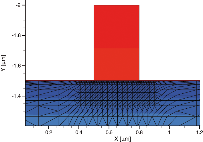
Figure 1. Placement of a refinement box: the extend argument extends the box beyond the mask edges, which are the edges of the polysilicon mask. (Click image for full-size view.)
2.4 Layout-Driven Contact Definition
At the end of the process simulation, contacts can be defined. This is usually performed by the etching of contact holes, the deposition of a metal, and planarization. Then, contact names are assigned to different parts of the metal. When using the Silicon WorkBench graphical user interface, it is more convenient to use the auxiliary layers introduced earlier:
icwb.contact.mask layer.name= ndrain  name= "drain"  point Aluminum x= -1.75
icwb.contact.mask layer.name= nsource name= "source" point Aluminum x= -1.75
icwb.contact.mask layer.name= ngate   name= "gate"   box PolySilicon \
  adjacent.material= Gas  xlo= -2.05 xhi= -1.95
Here, it is assumed that aluminum was deposited. With point Aluminum x= -1.75, the region of material aluminum that is found at a vertical position of x=-1.75 is converted to a contact (source or drain). For the gate, it is assumed that the planarization process removed the metal on the polysilicon, or no metal had been deposited on it. Therefore, the polysilicon–gas interface is defined to be the gate contact (see Figure 2).
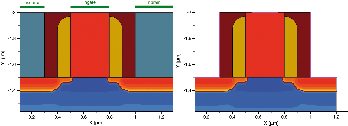
Figure 2. Layout-driven contact definition: (left) the structure after metallization and planarization, and the positions of the auxiliary layers are indicated by the green lines, and (right) the structure with contacts. (Click image for full-size view.)
main menu | module menu | << previous section | next section >>
Copyright © 2022 Synopsys, Inc. All rights reserved.